|
A tool chain is the sequence of operations (usually software) to go from the PCB design software inputs through to drilling, milling and exposing the printed circuit board.
Here is my tool chain development from Eagle 4.13 (an old but fully licensed professional version) Gerber and Exellon drill files to GBRL gcode. I’d rather not go through an intermediary image file (jpg or png) because this will almost certainly cause scaling issues subject to the raster size of the image.
From Eagle design your board. It is relatively standard to use imperial (inch) measurements for electronics as many components have pins and leads on multiples of 0.1 inche centres. Try and keep holes and vias on the overlay grid because Eagle Exellon will round to +/-0.001” which is about 5% of an 0.5 mm diameter hole.
Run the default exellon CAM job to produce an Excellon .drd drill file. When setting up the excellion CAM job make sure to de-select the positive coordinates option because this will add a computed X and Y offset to the drill file based on all layer geometry, and I haven’t been able to figure out the computation.
Now run the default gerb274x CAM job to produce the Gerber board layer files .cmp, .sol, stc and sts (and any others Gerbers that you might need).

Figure 1. Eagle PCB Design Software
FlatCAM seems to be a freeware package that will do what I want. It has a manual and there are lots of resources for the package on the internet. It will import Gerber and Excellon files directly, and with one critical tweak to the leading zero parameter and appropriate scaling for Excellon, everything is perfectly scaled.

Figure 2. FlatCAM Gerber and Excellon Processor
Drilling is defined in Eagle with an Excellon drill file. A problem is that Eagle Excellon uses 0.0000 inch format without leading zeros. In FlatCAM we need to execute the command:
After importing the .drd file we also need to apply a scale factor of 10 as FlatCAM is expecting to see Excellon numbers in the format 0.000 inch while Eagle produces 0.000 inch format.
Making the drill data (.nc) file was a breeze. My simple CNC Mill doesn’t do automatic drill bit changes so we’ll need a separate .nc file for each tool.
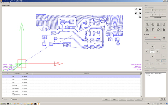
Figure 3. grblControl CNC Mill Driver
Making the laser data for each Gerber was a bit more challenging in order to optimize the tool path for speed and accuracy with an assumed 0.2 mm laser focal spot. This is a compromise between speed of area coverage, exposure and resolution. I can make a laser focal spot smaller than 0.1 mm, but even at moderate power settings it will likely burn the resist, and a larger spot means less time for exposure.
I ended up using the seeded paint option in FlatCAM because this entirely fills the non-copper painted regions with no artefacts or orphans and the beam is tight to the track profiles. This is not simply an isolation routing path but full exposure of all copper areas to be removed.
For working through the process I grabbed an old Eagle project file for a 3.3 Volt programmer power supply with current threshold monitoring. The double sided board is quite small at 30.5 mm x 22 mm but it has 22 SMD devices, 3 through hole components, and 20 drills. This will fine for developing the tool chain.
FlatCAM doesn’t seem to be able to a line-by-line render but in any case this is not particularly efficient as the laser spends most of its time turned off traversing space. I may have an issue with acceleration parameters of the stepper motor drives but this will require some experimentation.
The basic procedure is as follows.
Start FlatCAM.
From the Project Tab Import the Gerber file for a layer (.sol or .cmp for example).
Select the imported file.
Go to the Selected Object tab.
Scroll to Non-Copper Regions and Generate Geometry.
Go back to the Project Tab and select the generated object.
Go to the Selected Object tab.
Scroll to Paint Area
Set the tool diameter (0.2 mm), overlap (0.01 mm say), Seeded as opposed to Normal, and a margin of 0.
The following step is necessary for each contiguous area in the non-copper regions object including small thermal regions. Generate and then select a region in the Non-Copper Region Object.
With all regions selected go back to the Project Tab and use Shift and/or Ctrl to select all of the painted non-copper regions.
Go the Edit Tab and click Combine.
Go to the Project Tab and select the combo Object.
Go to the Selected Object Tab.
Set up the Feed to 1000 mm/min, Tool Diameter to 0.1 mm and Spindle to 100.
Now generate the Tool Path gcode and save it as <name.nc>.
I tested the .nc file by loading it directly into GBRL and sending to the CNC Mill. My simple experimental PCB job took just over six minutes to traverse the tool path. Even though the laser wasn’t connected I could see that it would have been active all throughout the job, and that we had some Z axis movement. Clearly with a laser we don’t want Z axis movement and we want the laser off when traversing between non-copper areas. The easiest way to resolve this was to parse the .nc file with a simple text editor (WordPad) and replace Z movements with appropriate laser on and off commands:
G00 Z0.1000 replaced with M05
G01 Z-0.1000 replaced with M03
The laser power is configured with a single gcode Sxxx command (where xxx ranges from 0 for off up to full on) right at the beginning of the file. This corresponds to spindle speed and adjusts the laser drive voltage accordingly.
I figure we want fast movement to stop stuff from burning so I’ll try 1000 mm/min initially. The gcode for this is F1000.
Note that for visualization of the laser path in the grblControl software that drives the CNC Mill we need to add some downward Z movement. G01 Z-0.1000 will do the trick for testing but this needs to be removed before actually doing laser exposures as it will change the point of focus.
Rather than make adjustments to every .nc file by hand I have written a crude but effective MSDOS batch file to automate gcode edits. The batch file stored in Parse.bat is:
@echo off
setlocal enabledelayedexpansion
::Replaces lines starting with Fx with Rx
::Ignores blank lines
::Output filename is @inputfilename
::Input file is preserved
set infile=%1
set outfile=@%infile%
echo. > %outfile%
set /A ctr=0
set F1=G00 Z
set R1=M05
set F2=G01 Z
set R2=M03
set F3=M03 S
set R3=S1000
set F4=F
set R4=F1000
for /f "tokens=* delims=" %%a in (%infile%) do (
set line=%%a
call :processline
)
echo.
echo %ctr% replacements made.
exit /B 0
:processline
set test1=%line:~0,5%
set test2=%line:~0,1%
if /I "%test1%"=="%F1%" (
echo %R1% >> %outfile%
set /A ctr+=1 ) else (
if /I "%test1%"=="%F2%" (
echo %R2% >> %outfile%
set /A ctr+=1 ) else (
if /I "%test1%"=="%F3%" (
echo %R3% >> %outfile%
set /A ctr+=1 ) else (
if /I "%test2%"=="%F4%" (
echo %R4% >> %outfile%
set /A ctr+=1 ) else (
echo %line% >> %outfile% )
)
)
)
exit /B 0
There are probably nicer ways of implementing this code as a batch file, and it could be much tidier in a higher level language. Given that I haven’t had cause to use batch file processing for years I’m just pleased it works.
Note that there are no blank lines in the original .nc file, and if there were then these would not be incorporated in the output file. The batch file needs to reside in the .nc directory, or its directory is incorporated in the path environment variable. Running the batch file is a breeze from the command prompt:
The original file remains unchanged. The parsed file is name @layername.nc, and this is overwritten if the script is run again. The batch files runs in just a few seconds and reports how many lines were changed in the original file. The file set for a double sided board is at least six files, of which four need to be parsed for laser exposure. Additional layers are required for every additional drill size, milling and vee notch operation but these don’t need to be parsed.
I’ll need another tool chain for building 3D milling gcode from STL models. MeshCAM seems to be the way to go here. It isn’t freeware but at US$250 for the entry level license this will probably do the job. However we don’t need to investigate this just yet.
My simple .nc gcode took about 10 minutes to prepare from the Eagle gerber .sol file and exposure took just over 6 minutes. This isn’t as bad as it might seem. While laser printing out two acetate masks doesn’t take long, these then need to be checked for print quality (toner spots and scratches) and errors, trimmed, aligned, reference drilled, cleaned, refitted, and both sides exposed. Provide that the new direct laser exposure actually works then I should have a significantly improved process – much will depend on how well the laser actually exposes the dry film resist (which still hasn’t arrived yet).
Oops, we have a slight problem. Dry film photo-resists are negative acting! The pre-sensitized boards that I have been using in my PCB process to date are positive acting.
Negative Acting: The exposed area is the area that remains.
Positive Acting: The exposed area is the area that goes.
I always need to think about this, even when I remember PLUS, ‘Positive Leaves Unexposed Solid.’
With native Eagle Gerber files the above procedure above works perfectly for solder stop masks, BUT NOT FOR THE TOP AND BOTTOM TRACK LAYERS. We need to expose the copper track areas, not the non-copper areas. So I need a way of inverting (making a negative) of the Gerber files. This is significantly different from mirroring.
My first thought was to find a simple way of inverting a Gerber file using the native Gerber Code. There are two Gerber parameters: %IPPOS*% and its inverse, %IPNEG*% and the layer parameter %LPD*% for Dark and its inverse %LPC*% for Clear. I tried changing these but they had no effect on the Gerber import into FlatCAM.
I tried a few other software tools such as Gerbv (which I have used forever for viewing Gerber files). The invert appeared to work on-screen but the resulting Gerber file refused to be inverted on FlatCAM import.
While I could go through a graphic or vector intermediate format I don’t want to do this for the reasons explained above.
My Eagle 4.13 software apparently inverts the Gerber of supply layers but I couldn’t get this feature to work at all, and in any case I don’t want to be messing with my existing Eagle design process.
Finally (after a lot more research) here is the FlatCAM method for producing negative Gerbers.
Import the Gerber into FlatCAM.
From the command console execute the command:
This produces an outline object of the solid features in the Gerber. We can now use FlatCAM paint as above to fill any region with a tool path object, combine these, and generate the final tool path for export as a .nc gcode file. This will generate a laser tool path inside the Gerber aperture features which means that the laser is now exposing the track and pad areas where we want the resist to remain.
I am making progress. The next mission is to experiment with the FlatCAM double sided PCB tool. This produces a mirror axis, mirrors designated layers, and produces arbitrary pairs of board alignment pin holes which are essential for turning the board over to expose the bottom (solder side) layer.
The tool took some getting used to. I suggest placing one of the alignment pins at (0,0) as this will allow easy alignment for changing between the mill and laser head. This may require the use of board offsets to ensure that the alignment pins are out of the artwork area.
Make sure that the arrangement of pins is only symmetrical about the mirror line to ensure that you can’t inadvertently turn the board around.
I suggest using the bounding box object in FlatCAM to assign the mirror line to get it exactly in the centre of the X or Y dimension of the Gerber.
I have settled on quite large 3 mm diameter locating pins because these will also be convenient for board mounting holes. While this may seem like a waste of board space, when making boards you want at least 10 mm of clearance around the board for handling, clamping and/or taping, and to avoid resist issues near the board edges.
Now I need a double sided PCB making procedure, if for no other reason than to have a standard process that I can adjust when I find that it doesn’t work! The procedure can be simplified for single sided boards by dropping the bottom layer resist coating, exposure, development and etching, but at least one locating feature is required to ensure alignment of the spindle and laser focal spot.
Place a flat sacrificial base board on the mill table and clamp it securely. Some folk use Perspex but 6 mm thick MDF should be flat over this table size, low cost, and it will machine (mill or drill) easily.
Fit a 3 mm drill bit to the spindle motor (to suite the locating pins).
Now turn the machine on and use the jog controls through grblControl to position the mill head to a convenient zero near the front left hand side of the sacrificial base. Turn the machine off and on again and the head is now at the XY origin.
Cut some FR4 board with a 10 mm (or larger) boarder than the finished board size.
Mount the blank PCB onto the board and clamp it securely, with the clamps well away from areas to be drilled or machined.
Load the pin drill .nc file, drill the alignment pins (at least four) say 6 mm deep into the sacrificial board, and any other 3 mm holes to a depth of at least 2.6 mm into the sacrificial board. If the non-locating holes are milled then the Z feed need only just cut through the board (say by 0.2 mm).
Push fit the locating pins into the sacrificial board.
Cycle through changing the spindle tool and drilling all other holes.
With the board drilled we can through-hole plate using either conductive ink or a copper ammonium complex to make the holes conductive followed by copper plating. While we could actually mask the board surfaces prior to plating I’m not sure if this is necessary yet.
Now Vee notch or tab mill the board outline and any cut-outs. We want to do all the machining operations before we start of the laser exposure.
If you’re planning on a quick isolation route now would be when the time for this operation on the top (component) side of the board. Then
For isolation routing flip the board and route the bottom (solder) side.
Clean the machine down, fit the laser head, and at a low power setting ensure that this is aligned exactly on the centre of origin locating pin. If necessary use the jog procedure above to re-zero.
Clean the board and apply photo resist film to both sides (for a double sided board).
Now tape it top surface up and expose the resist (component side).
Flip the board and expose the resist (solder side).
Develop the resist and etch the board.
A solder mask is not essential but it can be really helpful for keeping solder where it is intended to go, particularly for multi-pinned SMD devices with exposed tracks underneath, solder paste, and reflow. Clean the photo resist off the board, clean the board again, expose the solder masks on each side, and develop.
How easy is that? I don’t know yet but I’m about to find out. The first step is to experiment with the laser to work out what will effectively expose the resist layers for acceptable resolution and optimum coverage. Unfortunately this is on hold until my resist film arrives.
In order to do this I need to start applying some dry film laminate to bare boards. You can read about the Dry Film process by clicking on the link.
After some further experiments I have found that using the ‘Standard’ paint fill pattern in FlatCAM will work without artefacts (unexposed areas) provided that overlap, which is entered as % of line width and NOT mm, is at least 25%. This mode of fill is almost twice as fast as ‘Seeded’ despite what is effectively a a 25% double exposure over the majority of the paint area. My test pattern with 245 exposure areas (including lines, text, solid fills tracks and SMD packages) takes 11 minutes and 39 seconds for exposure at a traverse rate of 1000 mm/min.

Figure 4. Test Pattern
(68.55 mm wide x 53.01 mm high)
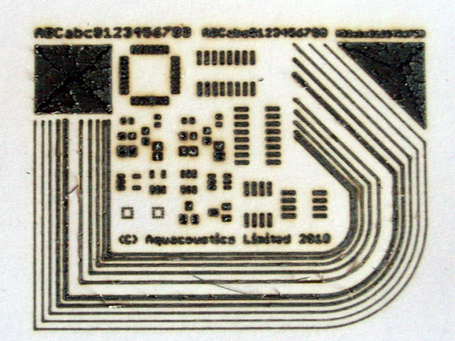
Figure 5. Test Pattern Exposure
(0.3 mm thick card at S 100 exposure, 1,000 mm/min traverse. Exposure time 11 minutes 39 seconds.)
I repeated the test at an exposure of S50. We are still getting 0.3 mm card burn-through particularly near the centre of exposed areas. But we can now expose 0.01” tracks and spaces reliably. We still have excess charring where there are small spaces between exposed areas but this is simply the nature of charring which will extend (bleed) beyond the actual exposed area.

Figure 6. Test Pattern Exposure
(0.3 mm thick card at S 50 exposure, 1,000 mm/min traverse. Exposure time 11 minutes 39 seconds.)

Figure 7. Test Pattern Close-up of Figure 6
(Clean exposure with no pixelation and 0.01” minimum line and spacing width.)
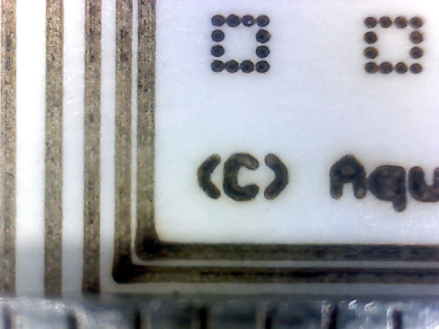
Figure 8. Test Pattern Close-up of Figure 6
(Some char-bleed evident between small features. Bottom graduations are 1 mm.)
After some experiments with dry film resist the laser direct exposure isn’t working very well due to flaring beyond the beam focal spot. But my original light box is working beautifully. However I need one more tool chain for producing Mylar film negatives on a laser printer for the light box exposure. Unfortunately the Eagle export command has an issue with how it handles via holes.
You can see from Figures 9, 10 and 11 that the Eagle tif export does not fill in the via holes. This is a problem because it will result in our via through-hole plating being exposed to the copper etch. I have experimented extensively with with layer hole fill settings and other options in Eagle to no avail. The only way I could get rid of the via holes in Eagle was to reduce the size of the via drill to an artificially low value (0.0001”, it does not allow zero) and reset the via diameter (off default). This is not a good procedure because it needs to be done on every via, and they do not necessarily have the same diameter.
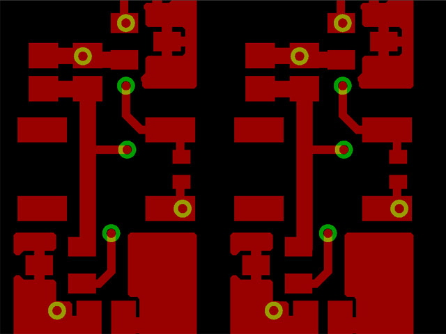
Figure 9. Eagle Component Layer (Screen Shot)

Figure 10. Eagle Gerber of Component Layer
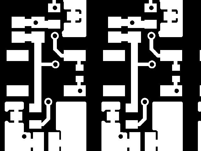
Figure 11. Eagle Tif Export of Component Layer
While more recent versions of CadSoft Eagle (I’m using 4.13) may have this capability I refuse to upgrade to a new product because the software is now owned by Autodesk and they have changed to an annual licence subscription model. In my opinion this is an Autodesk revenue generating exercise that does not provide value for money for infrequent users.
However there is a Windows 32 bit command line utility, Gerb2Tiff, available as freeware under GNU that will convert a native Gerber247x file directly to a default 2400 dpi image. The basic command line use is
The -b20 command line option adds a 20 mm background boarder around the Gerber file. The output .tif file from the Gerber at Figure 10 is shown in Figure 12. You can see that the via holes are now filled. The .tif image can be inverted and mirrored in your favourite image processing software and printed directly onto Mylar film at 2400 dpi.
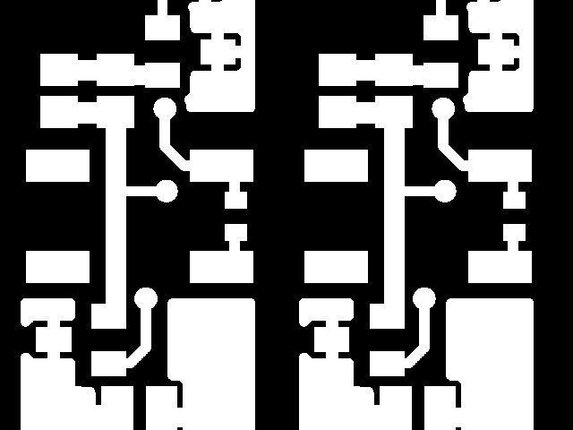
Figure 12. Gerb2Tiff Output from Component Gerber at Figure 10
So the tool chain for producing light box Mylar negatives from Eagle 4.13 is:
Run the Eagle CAM job gerb247x on your board layout.
Run Gerb2Tiff on the component, solder and solder mask layers.
Invert the all of the .tif images and horizontally mirror the component layers.
Print the Mylar negatives at 2400 dpi.
|