|
Putting it all together…
Design your board using your preferred program (in my case CadSoft Eagle 4.13). This board is for my green 100 mW laser modules with adjustable thermal compensating current regulation, wider supply voltage tolerance, and reverse bias protection. This board is just 22 mm long.
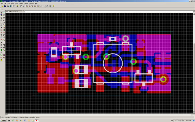
Figure 1. Board Design in Eagle
Double check your component footprints and clearances, and hole sizes. All vias on this board are to be drilled at 0.6 mm and there are no through-hole components.. Try and stick to as few drill diameters as possible as each will require a change in drill bit size.
Run the error check to make sure that the schematic and board are consistent. Errors may be tolerable provided that you understand what these are. Often times I deliberately connect IC supply pins to arbitrary supply rails which generates tolerable errors.
Run your board design rule check. Again, errors may be tolerable. On this design I have deliberately placed some vias on component pads to save board space. This is not good design practise but it is tolerable in this design.
Turn the board into a panel. I only need five boards but I can do six using the same board area. Allow enough space between each board to allow for cutting or milling separation. Add say 10 mm all round for clamping, handling, and mask overlap, but at least 50 mm at the top for mounting in the plating tank. This gives me an overall panel dimension of 65 mm wide x 90 mm high. Place the home position at the bottom left of the panel to aid CNC alignment.
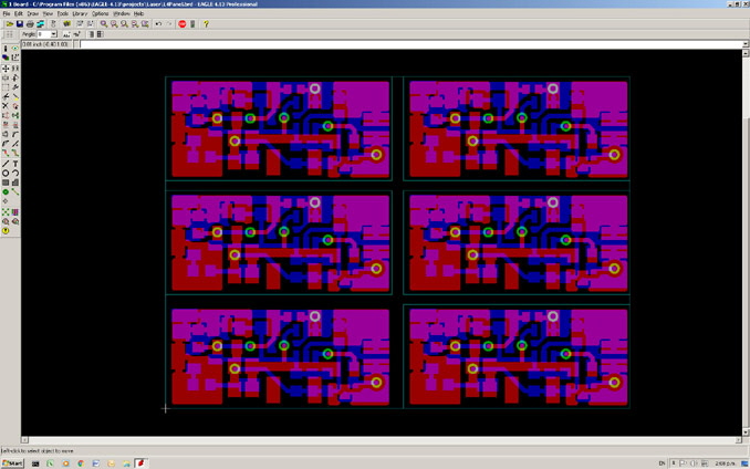
Figure 2. Panel Layout in Eagle
Run the Eagle Gerber247x and Excellon CAM jobs to produce the drill file and the base Gerber files for processing into negatives. The files that you’re going to need have extensions .drd, .cmp, .sol, .stc and .sts using the default Eagle extensions. They define the drill file, the top component layer, the bottom solder layer, the top component stop mask, and the bottom solder stop mask.
Convert the Gerber files to .tif graphic files at a resolution to suit your printer (1200 dpi or higher recommended) using the command line utility Gerb2Tiff with a 10 mm boarder.
Open the .tif conversion files in an image processing package (I use Adobe Photoshop), invert the component and solder layers (not the solder mask layers), horizontally mirror the two component files, scale to correct for size, save and print to Mylar film at the .tif resolution used to produce the tif files from the gerber files. If the toner layer isn’t solid or flakes off the Mylar then increase the paper thickness in your printer settings. You might also want to print a paper copy of the solder layer to act as a guide for setting up the CNC drill.
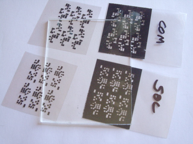
Figure 3. Artwork Printed
Cut the printed circuit board to the panel size (calculated above) with margins for handling.
Convert the .drd file into a CNC machine control file using FlatCAM. Set the panel on the mill with a suitable sacrificial bed (I’ve used 5 mm thick MDF). Fit an appropriate drill bit, align the zero, double check the orientation and dimensions to make sure you’re not going to run out of space. Run the machine file to drill the panel. Remove any burs.
Clean the board and activate it using a copper based activator. Silver based activator seems to produce better plating but causes problems during etching. Avoid handling or excessive cleaning of the activated board.
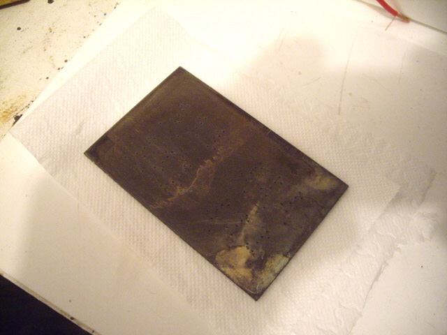
Figure 4. Activated Board
Complete the through-hole plating and inspect for visible plating errors. Buff the board surfaces back to flat and bright. Then clean and dry.
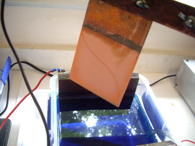
Figure 6. Through Hole Plating
Apply dry film resist to both sides of the panel. Align and fix the artwork prepared above using adhesive tape positioned clear of the image. The toner side of the Mylar film goes against the copper. Use the holes for accurate alignment. Expose and develop. Now remove the art work, noting that the protective resist layer is likely to come off with the artwork. Trying to remove it when it isn’t actually there is clearly not possible and you will chip the resist layer.
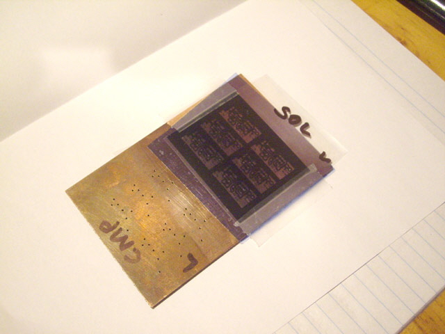
Figure 6. Resist Layer with Artwork Aligned
Inspect the dry film. Check for any broken tracks, shorts between adjacent conductors, and proper tenting over any holes to ensure that they are completely sealed to the board. If necessary the film can be carefully scraped off after the protective layer is removed to clear shorts, and any accidentally exposed areas can be coated with a resist pen or nail varnish, but this will likely produce a tacky finish.
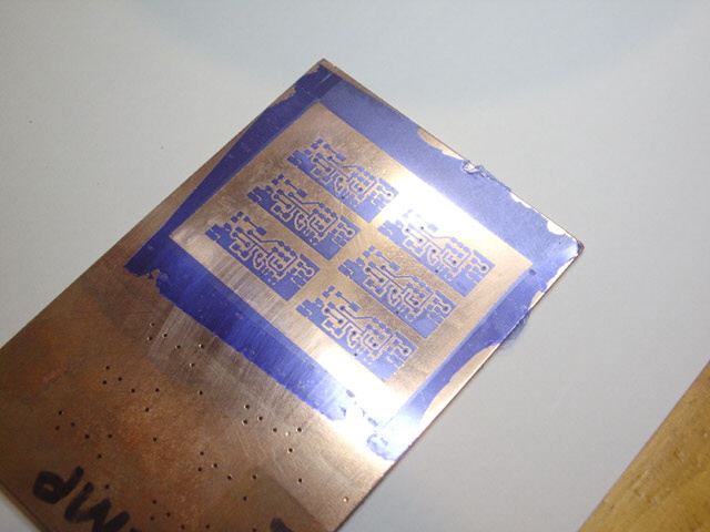
Figure 7. Resist Developed
Etch the panel using your preferred etchant. Remove the resist in Sodium Hydroxide (10 g / litre), rinse and dry. During etching the silver activation layer seemed to be quite resistant to the Ammonium Persulphate etch. This required excessive time in the etchant and gentle scrubbing with a tooth brush resulting in undercutting of the resist and one damaged track.
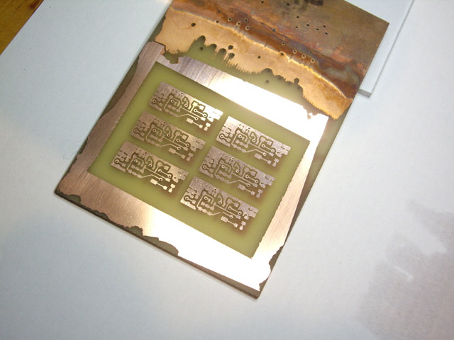
Figure 8. Etching Done
Inspect the panel checking for electrical continuity on conductive paths and between layers, and short circuits between tracks. I had just one broken track which was caused by scrubbing and over-etching, required because the silver activation layer was resistant to the Ammonium Persulphate etchant, and one potential track short, again due to the persistence of the silver activator. All of the through holes were a dead short between layers.
Clean the board with acetone or isopropyl alcohol and bake dry in a convection oven for 30 minutes at 120°C. Apply the solder mask dry film to both sides, align and fix the artwork with toner side to the copper. Expose, develop, cure and bake in accordance with the manufactures directions to harden.
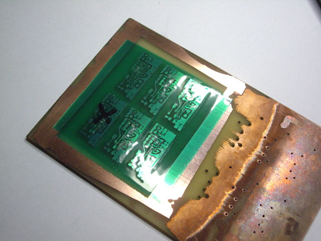
Figure 9. Solder Mask Dry Film Applied
f you want to plate the terminations with Tin now is the time. I use proprietary tin plating crystals.
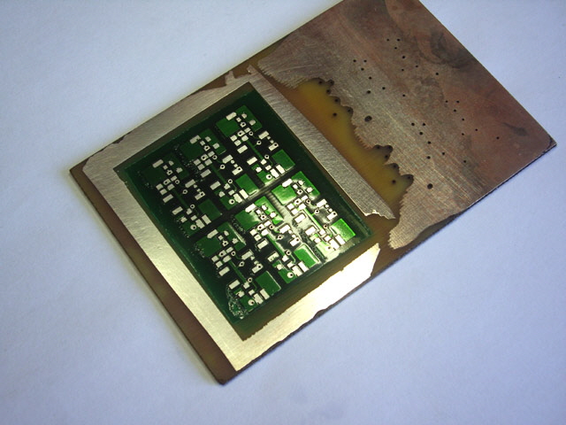
Figure 10. Tin Plated
The final step is to cut the boards from the panel. This might be a milling operation, but 99% of the boards that I’ve ever had cause to make have been rectangular and I can do this by hand using my small guillotine in about a minute for moderately sized boards. Really small boards like these ones are challenging with the guillotine and you will probably need to do some hand filing.
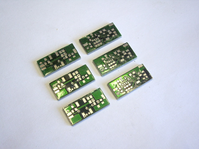
Figure 11. Boards Cut to Size
All going well you should have a nice through-hole plated prototype board with solder mask ready for assembly.
The solder masks make for easy hand soldering of even the smallest components, with virtually no risk of inadvertent solder bridge short circuits between pins or beneath packages. Any balled excess solder paste is easily removed with a deflux using Isopropyl Alcohol.
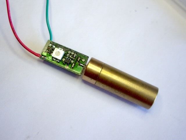
Figure 12. Assembled and Tested
On assembly and testing there were two problems with this particular prototype board. The first was that I had used 1.6 mm thick FR4 which was too thick for edge mounting a 5.6 mm laser diode. The second was a design issue to do with the on/off push button when operating above 3 Volts. So I’m going to be remaking the board which is the very reason for having the ability to prototype in house. While these boards are small they would take maybe a week or so from a board house at considerable expense for what is essentially scrap. I can remake, populate and test the new boards in a day.
20 January 2019 and the process sill isn’t quite right. While the dry film process and exposure is working consistently, by the through-hole plating is still less than perfect, and it seems to be causing issues with etching. A test etch with HCL H2O2 stripped an unplated sample baord in just 3 minutes. Fast is good because it stops under-cutting. But the etch process on a through-hole coated board stalled at the through-hole layer and thereafter was effectively poisoned (ruined). This isn’t good and I need to revise either the through-hole activation or use an additional mask process to keep the activating solution off the bulk of the copper.
More to follow...
|