|
I’ve had a few hits on Turtlesarehere.com for information on making double sided PCBs so here is the process I use. It is good for single sided boards too. It will take at least a couple of hours, and maybe longer depending largely on how many holes you need to drill, but you can produce high quality boards with tracks as thin as 0.1 mm (less than 5 thousands of an inch), and even better registration between layers. See Figures 11 and 12 at the end of this page to see just how good your board can be.
A question you might ask is ‘why make my own PCB when there are lots of companies that will make your board using your artwork at reasonable prices and with relatively fast turnaround?’ My experience has been that making-your-own is always a faster and cheaper option for one off boards. For prototypes home made lets you test your design for layout issues like wiring errors, noise susceptibility, oscillation, component package sizes, ease of assembly, et cetera before committing to commercial production. In the development of my Amigo I have made this mistake on two occasions where I sent a board design directly to a manufacturing company in the hope that the design was right. They made me exactly what I asked for and despite their perfect product I wasted several hundred dollars and two weeks making PCBs that are only good for beer coasters - let me know if you want one. Actually they are too small for beer coasters so they are consigned to scrap!
Before you start making your boards two good references are ‘Making Printed Circuit Boards’ by Jan Axelson, ISBN 0-8306-3951-9; a relatively elementary, but straight forward text; and ‘The Circuit Designer’s Companion’ by Tim Williams, ISBN 075061756X; a serious text with everything you ever wanted to know on the subject including layout (and a whole lot of stuff that you probably don’t want to know about). There is also some great material on the web including Mike’s Electric Stuff.
Make your artwork. I use Eagle Version 4.13 Professional PCB software from Cadsoft. Make sure that: everything is connected (use any design rule checks that your software has), that the component packages are the right size, that you have provided adequate separation between tracks for voltage, and the tracks are appropriately sized for current. I make all holes with an 0.1 mm diameter drill centre-mark to ease manual drill drill alignment. Small drills will bend just a wee bit before they break! As a general rule keep tracks short, wide and direct to avoid track inductance which causes signal transients to ring. Avoid sharp bends - these are often-times a cause of track corrosion. Try and cover as much copper with resist as you can - with appropriate grounding (ground planes) this can significantly reduce coupling between signal tracks and saves on the consumption rate of enchant.

Figure 1. Making the Artwork using Eagle
Modern PCB layout software packages and laser printers are a huge advance on the old days of using Bishop decals and tape to painstaking layout the tracks by hand on film and reduce these using photography. With software when you’re through with development and making your prototype you can submit your design to a board manufacturing facility. There are a number of packages, including Eagle, available for free on the net (although usually with limited board area, layers and components).
Include at least three fiducials (alignment marks) on all board layers. These should be as far apart as possible. If you have critical alignment components (SMD processors with fine pitch connections for example) then you might want to put a fiducial mark beside these too. I assure you they will help with alignment.
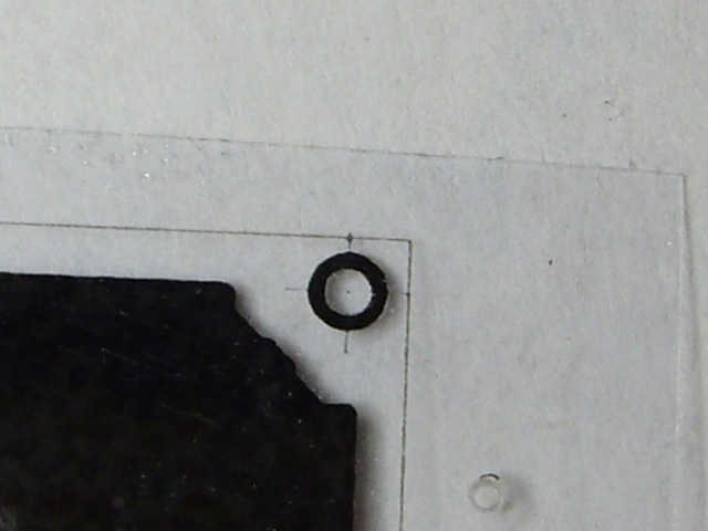
Figure 2. A Fiducial (and an Alignment Hole)
Print the top and bottom artwork onto overhead transparency film using a black and white laser printer of at least 600 dpi. Make sure that you mirror/rotate the images of both layers so that the toner side of the image will be against the board during UV light exposure. I use positive-acting presensitized FOTOBOARD2 board so my artwork looks like the tracks that I’ll be producing. You can sensitize your own copper laminate boards using products like Electrolube PRP. I have found the extra time, mess and expense is not worth the effort unless you are trying to do something exceptionally clever (like etch text onto a metal goblet). Presensitized boards ensure consistently excellent results.
Figure 3. The Printed Artwork
Note that overhead transparency film distorts when it’s printed due to the printer fuser roller heating the film. Make sure that the artwork is in the same orientation on each page so that the any distortion of the film will be similar on the different layers.
Inspect the artwork. Look specifically for any defects in the track detail (caused by irregularities in the toner) and extra spots of toner. Keeping your grubby fingers off the artwork. Cleanliness is really important. You don’t want dust on the artwork, nor do you want to damage the toner image.
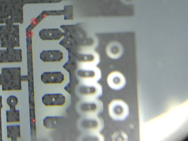
Figure 4. Some Nasty Toner Bubbles under the Magnifying Glass (Red Highlight)
Time to Reprint the Artwork
Cut some presensitized board to at least 10 mm larger than the circuit image. I use a fine toothed hack saw and lightly file the edges to remove any burrs - but a guillotine is much better. Clean the board of any dust/swarf, leaving the light-protective film in place for now. The 10 mm clearance will give you some handling area and prevent the use of the extreme edges of the PCB (where sometimes the light sensitive coating is less than perfect). Handle the PCB with care to avoid damaging the light-protective film, sensitized coating and the copper laminate.
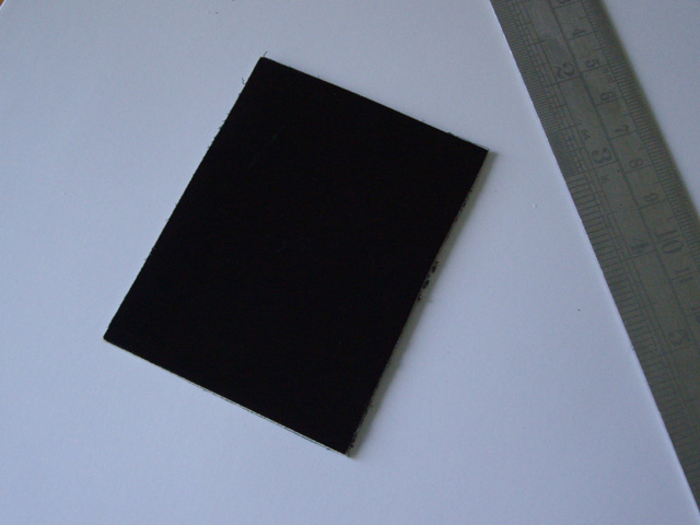
Figure 5. Presensitized Fotoboard Cut to Size
Now trim the artwork with scissors so it is a few millimetres smaller than the cut board, and with the toner images together, align the artwork using the fiducials on one side of the board. I use a small piece of Perspex on top of everything to ensure the artwork is dead flat, a piece of white paper between the artwork and the presensitized board so I can see the fiducials, and a magnifying glass. When the artwork is perfectly aligned use adhesive tape to attach it directly to presensitized board.
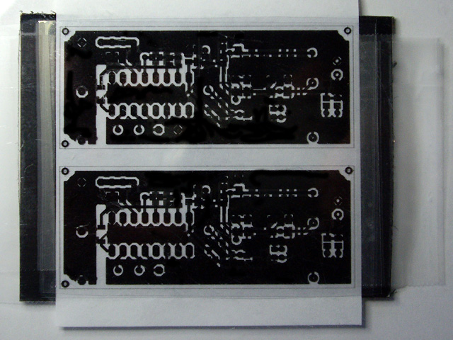
Figure 6. The Artwork Aligned and Taped to the Board
Again using a sheet of Perspex to keep everything flat, I drill 0.7 mm diameter holes at each of the corners of the board. The holes must pass through both layers of the artwork film and the presensitized board. Their exact location is not critical but you want them as far apart as possible and about 5 mm from the edge of the board. These will be the alignments for positioning the artwork before UV exposing the board.
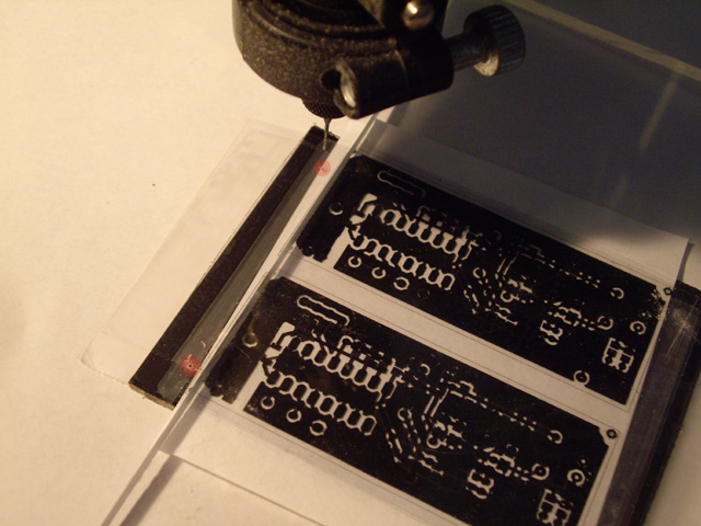
Figure 7. Drilling the 0.7 mm Diameter Alignment Holes (Red Highlight)
Clean everything by gentling wiping or blow-brushing the presensitized board and the edges of the artwork. This is necessary because any drill swarf could scratch the image, or mask clear parts of the image, or prevent the image from sitting dead flat on the board during UV light exposure.
Orientate the board with one piece of the artwork (toner side to the board). Now, in subdued light, remove the light protection film from one side of the board, place the artwork onto the sensitized board surface, and accurately align the 0.7 mm diameter holes. To ensure accurate registration of the layers I use sewing pins placed through the drilled 0.7 mm registration holes in the board and the artwork and a piece of Perspex to ensure that the artwork is dead flat with the board during alignment. Tape the artwork to the board at the edges, avoiding putting the tape over the circuit.
Now expose the board to UV light. Past experience has taught me that my light box and Fotoboard require no more than an 105 second exposure but you may have to experiment with some test strips for your set-up. The Fotoboard resist changes from a greenish/yellow to clear when it has been correctly exposed. Once exposed leave the artwork taped to the board to protect the surface from damage or unintentional light exposure.
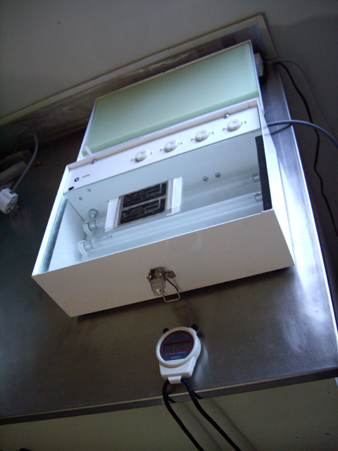
Figure 8. Exposing the PCB to UV (Second Side)
Orientate the unexposed side of the board with other piece of artwork (again toner side to the board), remove the light protective layer from the unexposed side of the board, and using the sewing pins, align the 0.7 mm holes and tape the artwork in position just as you did for the previous layer. Then expose this side to UV too.
Remove the artwork from the exposed board and develop it. I use a sodium hydroxide solution (12 g/litre) at about 25°C although other folk have have found this to be too unreliable and use proprietary solutions. The temperature of the developer is very important. If it is too hot it will strip all of the resist from the board before you can blink. If it is too cold then you will end up having to force-etch resulting in undercutting and failure of thin tracks. The developer solution seems to last forever. Mine is three years old and still going strong. Wear gloves and glasses. The board should take between 40 and 60 seconds to develop leaving clean red/pink bare copper where the resist has been exposed. After about 25 seconds you should see a black residue coming from the board - this is a good sign but development is not complete. Wait another 15 seconds or so to allow the resist between fine detail to dissolve. Rinse the board in cold water when it is developed to stop the process.
Inspect the developed board, handling at the edges only. Look for damaged tracks or marks in what should be clear copper. If necessary these can be reworked using an etch resist pen and a scalpel.
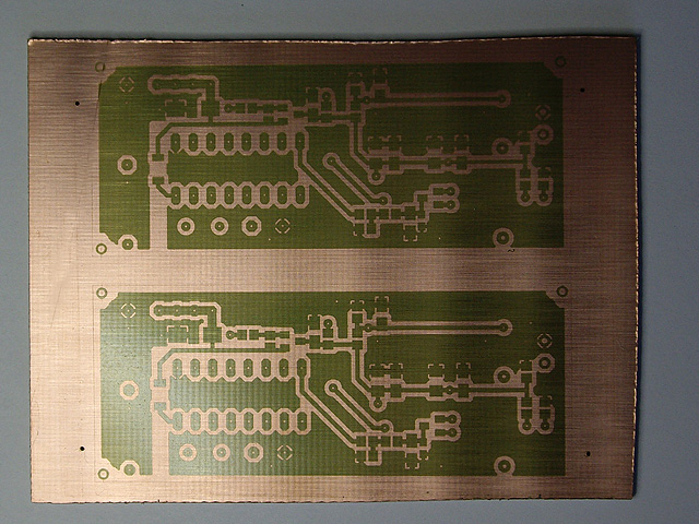
Figure 9. A Developed (and Inspected) Board
Now etch the board. Wear some disposable rubber gloves and eye protection. I use ammonium persulphate solution (200 g/litre) at about 75°C. I pour my 1 litre stock solution at room temperature into a plastic ice-cream container and heat it in the microwave for about 4 minutes. Etching takes about 8 minutes with fresh etchant, but up to about 15 minutes with older/used solutions. If it takes longer then it’s time to make up some fresh solution. If the exposed copper doesn’t look salmon-pink when lifted-clear of the etchant within the first few seconds then the board has been under exposed or under developed. You have stuffed up and will need to start again after doing some exposure test strips. Be assured that most people that want to make PCBs have been here.
Be aware that too long in the etch will cause tracks to undercut making the edges ragged and the tracks thinner than planned. This is not good. Avoid it by removing the board not more than a minute after the last visible copper has been etched. Wash the etched board with detergent, rinse and dry before inspecting it again for track damage and to ensure that all of the copper has been removed between lands, tracks etc. If there are errors then you can remove copper with a scalpel but repairing tracks requires specialist gear to make a good job. This is kind of like cutting timber to size - you can always cut more off but you cannot cut more on.

Figure 10. Etching - Note the Salmon-Pink Copper and the Alignment Holes
Time to drill the board. Make sure the the drill press is aligned so that the drill is perpendicular to the board. I have finally dispensed with drill alignment by eye as too time consuming and inaccurate. I now drill all holes directly to size using a Dremel press with a below mounted self-illuminating USB microscope with 15 times magnification. You need one of these. Click here to see how you can make one for just a few dollars in half a day. Hearing and eye protection are a must. Inspect the board to make sure that you haven’t missed any holes and that the holes are the right size. Don’t forget the PCB mounting holes if you need any. Trying to drill a board when it is populated with components is a pain and can quite easily damage the components.
Now I cut the board to size and file the edges flat taking care not to damage the copper. One day I must invest in a PCB guillotine. And the result of your hard work? click on the link for an image showing just how good the registration between the layers can be.
Tin plating is not essential but it can make SMD hand-soldering a heap easier and makes for a professional looking finish. However be aware that modern photoresists often act as fluxes and provide a good protective layer over the copper tracks. If you want to tin plate the board then clean the resist off the board. Ethanol (methylated spirits) works well with Fototboard. When the resist has been removed lightly scrub the board with a kitchen scourer to remove any raised copper drill lands and remove any oxide from the copper. Once the board is perfectly clean keep your fingers off it. I use a proprietary tinning solution ‘Tin Plating Crystals’ from RS Electronics (90 g per litre) at a temperature of around 20°C. The made-up solution doesn’t keep too well (say six months maximum) and old solution will not give a bright tin finish. With gloves on I place the cleaned board in the tinning solution and move it around every few minutes for 20 minutes. Then rinse the board with hot water, wash it with detergent, dry it with a paper towel and gently buff it with paper towel to make the tin shiny. All done!

Figure 11. A Shiny Tin-Plated Double Sided PCB Drilled and Ready for Soldering
A word or two on soldering to chemical tin plating. Use self-fluxing solder and avoid an extremely hot iron or long periods of heating or you will damage the tin plate. If this happens then tin the exposed copper with solder. If the board has been sitting around for more than a few days before being populated (or requires some other soldering after a period of time) then either rebuff the tin using a paper towel as described above, or using a rubber pencil eraser, gently rub over the lands to be soldered to remove any surface oxide.
Connecting a conductor on one side of the board to the the other is done professionally using through-hole-plating. This process is difficult to do at home so I use either leaded components or Favorit copper rivets (Mega Electronics) soldered to each side of the board. As a general rule making through connections underneath components (like an IC) is a dumb idea because they are impossible to re-work without removing the component. Don’t say I didn’t warn you! It’s a good idea to check each connection with an ohmmeter before you start assembling the components.
Hopefully this has been instructive to someone out there and helped to produce a professional and functional double-sided printed circuit board. Please use the contact me page if you have any suggestions or questions.
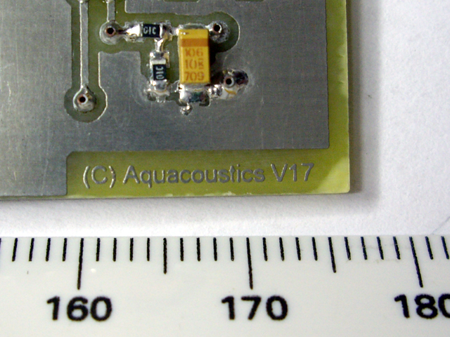
Figure 12. Resolution. Graduations are 1 mm. Awesome!
|