|
I’ve picked up this project again after almost two years of gathering dust.
There are some aspects of my initial design approach that I don’t particularly like so I have started from scratch (and rewritten this page) based on the use of the AD630 as the Lock In Amplifier (LIA) and addressing phase control directly through the microcontroller.
My original applications included both molecular oxygen calorimetry and oxygen sensing for SCUBA rebreather apparatus. The second of these poses some significant challenges as the absorption peaks spread at increasing pressure to the extent that individual peaks cannot be discerned at 10 bar. However the fundamental Beer Lambert law should still hold. The attenuation of the merged band should still decrease as the oxygen concentration reduces. However this will require consideration of the pressure of the sample.
A significant issue with this project is sourcing a low cost VCSEL or DFB single mode laser diode operating at 760 or 763 nm. These devices are expensive (ranging from several hundred to several thousand dollars each) and there are only a handful of manufacturers.
The lasing frequency and emission bandwidth are important. The frequency needs to be in the vicinity of oxygen absorption bands and away from other stuff (N2, CO, CO2, H2O, etc) which might mask the signal that we are interested in. The laser also needs to be tuneable over say 1 nm to allow the band to be scanned over perhaps two or three absorption lines.
I have three VCSEL 763 nm lasers on order.
Signal Basics
Before I get too carried away there are some signal basics that I need to consider.
The VCSEL lasers have a current tuning range of 0.6 nm per mA, over a current range of 0.5 (lasing threshold) to 2 mA maximum output. The corresponding output power varies from 0.0 to about 0.7 mW and has a linear characteristic with temperature and current. I figure to operate the laser between 1 and 2 mA. It is rated at modulation frequencies up to 100 MHz so there will be no discernible loss in output power at a few kHz. The typical beam divergence is about 17 degrees so I will probably need some collimating optics.
The PIN photodiode is matched with the laser for peak sensitivity at 760 nm with a relatively flat response over tens of nm. The device has a very low capacitance of just a few pF so it will be fast (rated at 1 GHz). The output is rated at 0.51 A/W.
So we can expect a PIN photodiode current in the range of between 150 and 350 uA from a lasing current of between 1 and 2 mA with corresponding laser peak emission frequency of between 762.7 and 763.3 nm.
I have selected a modulation frequency of 1 KHz because this is optimal for the AD630 LIA. But how much modulation (modulation depth) should be applied?
Modulation Depth
This single parameter is probably the most critical to the success of the design. It determines the frequency shift of the laser and must be sufficiently small to resolve the molecular oxygen absorption peaks (and their first and second differentials). However as the modulation depth decreases so does the LIA output which will be detrimental to the signal to noise ratio.
Using the AD630 we can expect to recover modulated signals of known phase and frequency embedded in 100 dB of noise (signals 100,000 times smaller than wide band random noise).
Oxygen absorption peaks of air at Standard Temperature and Pressure (STP) in the 763 nm band are around 0.125% of the base line and they are very narrow. The Full Width at Half Maximum (FWHM) is less than 0.006 nm (using the Voigt profile to account for pressure broadening and Doppler effects).
Because our modulation scheme is digitally based we assume that the laser modulation will be a factor of 1 mA (the scanning range) divided by 2n. I have used an Excel spreadsheet to determine that n = 512 will provide a good compromise between absorption peak resolution and signal output. This gives a laser modulation depth of about 2 uA.
Note: Traditional TDLAS techniques use sinusoidal modulation which results in continuously varying laser intensity and frequency. The optimal modulation depth for these systems, assuming Lorenzian absorption line shape, is understood to be 2.2 times the FWHM line width. This corresponds to a sinusoidal laser modulation current of about 22 uA ppk. For now I will persist with my digital modulation scheme because I suspect that it will have significant advantages in frequency control, modulation depth control, the demodulation scheme and signal measurement. If I have got this wrong (and I may have) then I can always revert to sinusoidal modulation.
Laser Drive
The first stage in the new design was developing a microprocessor controlled current drive for the laser. It needs to provide fast switching with minimal overshoot with a resolution of 2 uA between 1 and 2 mA. This corresponds to a resolution of 0.0012 nm over an 0.6 nm tuning range providing about 20 samples across an absorption peak.
The voltage drive comes from the microcontroller via a Digital to Analogue Converter (DAC). I’ll be using an R-2R DAC design driven directly from an 8 bit port and an extra IO pin to get the 512 bit resolution.
Here is my laser drive circuit.
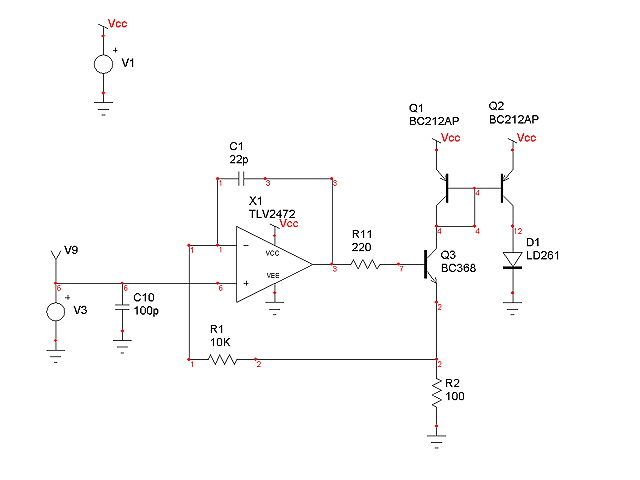
Figure 1 Laser Drive
The op amp, transistor Q3, and resistor R2 are a classic transconductance (voltage to current ) amplifier. Transistors Q1 and Q2 form a current mirror to provide a high side drive to the laser diode, D1, so I can keep the case grounded. With R2 = 1000 Ohms and other component values as shown the drive output is ~1 mA/V, readily adjustable by tweaking R2.
The circuit has inherent current limiting of about 3.8 mA from a 5 volt supply due to the 2 Vbe drop of Q1 and Q3 in series with R2.
While I am waiting for my lasers to arrive I am using a 960 nm GaAs IR LED (why destroy an incredibly expensive laser when I can destroy a low cost LED instead) with an appropriately matched PIN photo diode.
For testing purposes I have arranged an LM555 timer and a simple resistive voltage divider to provide an output current of nominally 2.5 mA modulated with a 2.5 uA, 1 kHz square wave. The actual LED current was measured at 2.12 mA modulated with a 1.85 uA square wave with a rise and fall times of about 100 ns from 10% to 90% with minimal overshoot and ringing.
There are several reasons why the actual output current is different from the calculated value. These include the input offset voltage of the op amp, the precision of R2 (2%), the fact that Q1 and Q2 have not been matched, and the inherent loss of Q2 base drive in the current mirror.
In my test circuit there is also an appreciable quantity of high frequency noise. I figure that most of this is due to my breadboard layout (and the use of a breadboard in the first place), a ground loop between the power supply and my oscilloscope, and a complete lack of shielding.
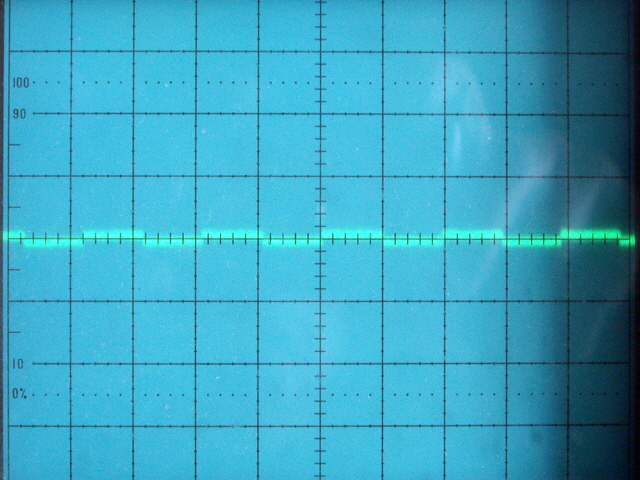
Figure 2. Modulation Component of LED Drive Current
Vert. 20 uA/Div. Horz. 0.5 ms/Div
During testing I had one minor disaster. One of the supply leads inadvertently contacted something it shouldn’t have and the op amp blew to bits (literally). Bugger! I replaced the op amp and have gone to some lengths to avoid accidentally shorting stuff in future.
PIN Photodiode Amplifier
The receiver design has some demanding specifications. It needs to be fast, accurate and low noise.
A classic transconductance amplifier is a good starting point for the design with the PIN photodiode operating in photoconductive mode for switching speed. The significant and constant negative bias across the photodiode reduces its capacitance allowing for fast switching. This can be further improved by adding a common base transistor at the input to form a hybrid amplifier that reduces the Millar effect.
For testing I have used a PIN photodiode that has a matched peak response at 960 nm with my test LED emitter. This component has a relatively high capacitance of about 70 pF so I anticipate that its switching performance will be relatively slow.
The basic circuit works well with a gain of ~ 220,000 V/A (established by R12) but the high standing current of the illuminated PIN photodiode and the relatively high gain causes the output to saturate. However we are only interested in the small modulation component of the signal. To remove the DC bias component I have added a servo which consists of a highly damped low pass filter, a slow integrator (the servo) and a common emitter transistor with degenerative emitter feedback to provide the DC bias at the inverting input of the operational amplifier. Note that the low pass filter cannot be a simple passive RC filter because the integrator sources or sinks current which changes the DC.
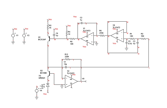
Figure 3. PIN Photodiode Amplifier
(see Figure 14 for an improved implementation)
The design provides up to 200 uA of DC feedback which should ensure that the output will servo to 0 V DC under all anticipated input light conditions.
The circuit is necessarily highly damped to prevent oscillations when the bias level changes and to prevent droop distortion of the signal component.
In my test circuit I have used a TL071C JFET input op amp for the transconductance amplifier and an LMC6482 dual op amp for the servo. In future designs I’ll be changing the TL071 for a device with a lower noise figure.
On power-on the circuit settles to the quiescent state in about 250 ms. When driven by the LED transmitter the output waveform is a 1 kHz square wave with minimal overshoot and just a small amount of droop. The droop is actually a test circuit problem as I have used 0.1 uF capacitors because I don’t have leaded 1 uF non-polar capacitors that I can use on the breadboard. With the LED and PIN diode closely coupled the amplifier is producing about 10 mV output from 1.85 uA LED modulation and the circuit is dead stable about ground despite operation in ambient daylight with no optical shielding of the optical path!
The rise and fall times are satisfactory, particularly given my low speed test PIN photodiode. There is a significant transient on switching which is being coupled from the transmitter via the power supply (yet another breadboard layout issue probably combined with inadequate supply decoupling).
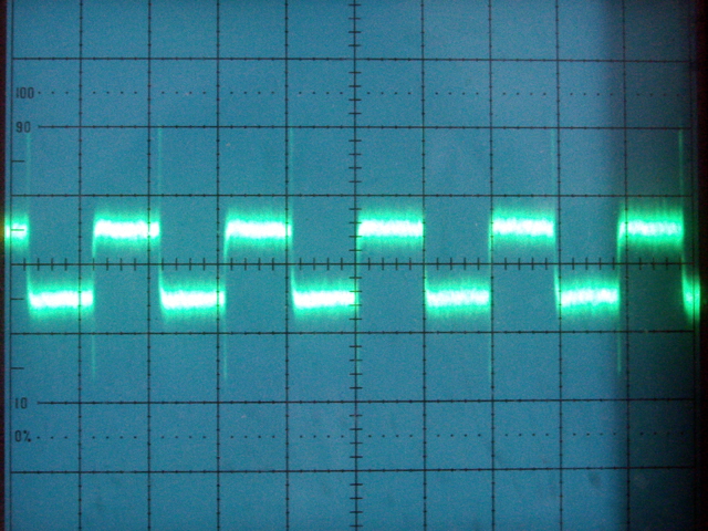
Figure 4. Amplifier Output from 1.85 uA LED Drive
Vert. 10 mV/Div. Horz. 0.5 ms/Div
It is interesting to compare the performance of my IR LED and 960 nm PIN diode with my proposed VCSEL laser and matched PIN diode.
Figure 4 shows a peak to peak modulation frequency output voltage from the PIN diode amplifier of about 10 mV. The corresponding modulation current in the PIN diode is about 45 nA corresponding to about 2 Lux. The LED output is rated at 1000 Lux for a forward current of 50 mA, dropping to a relative output of 0.01 at a forward current of 1 mA. Further the output power reduces with increasing frequency and is about 0.2 at 1 kHz. So our LED modulation output is about 1000 Lux * 0.01 * 0.2 = 2 Lux. The LED and the PIN diode are closely coupled so we can pretty much ignore beam angles.
My lasers (which have arrived and remain sitting in their electrostatic protection until the electronics is transferred to something a little more permanent that breadboard) are rated at an output of 0.25 mW at 1 mA with a slope of 0.5 W/A. So our 2 uA modulation current should produce about 1 uW. For now let’s assume that I have incorporated collimating optics to reduce beam spread.
The matched spectral response (760 nm) PIN diodes are rated at 0.51 A/W. So we expect a modulation PIN diode current of current of 1 uW * 0.51 A/W = 0.51 uA. Now we apply the gain of our PIN diode amplifier at 220K V/A to get an output of about 0.1 V or about 10 times greater than our IR LED and PIN diode shown in Figure 4.
Lock In Amplifier (LIA)
Time for the LIA. The basic design is directly from the Analogue Devices AD603 data sheet, but with an improved performance low pass filter, additional gain, the facility for DC offset, and my digital modulation scheme. The additional gain and DC offset are required to ensure that the output will fully utilise the dynamic range of my analogue to digital converter.
As previously mentioned most traditional TDLAS designs drive the laser with a relatively slow ramp (say 100 Hz) with a small sinusoidal modulation at about 40 kHz. The LIA demodulation frequency is typically chosen to detect a harmonic of the modulation frequency to extract the absorption peak differential or its double differential. The performance of these systems is reportedly much improved when demodulating at the harmonics which are large enough for detection and have the added advantage that the output automatically establishes a horizontal base line.
My square wave (digital) modulation scheme is based on developing these differentials through time-averaged finite differences of the synchronously demodulated signal. A potential advantage of digital modulation is increased harmonic strength for recovery of the differentials and increased gain. The reason for the increased gain is that the integral of a rectified sine wave is the RMS voltage (0.35 times the peak-to-peak amplitude of the unrectified signal). Where as with digital modulation the integral is 0.50 times the peak-to-peak amplitude.
What follows is an Excel simulation of the anticipated performance of my modulation scheme. I have estimated the absorption line as having a Gaussian shape with a typical with a peak absorption of 0.00125% (typical for molecular oxygen at Standard Temperature and Pressure). You can see that the signal levels that we are playing with are relatively small hence the requirement for an LIA.
Note. Figures 6 and 7 have been updated on 23 October 2014 due to an error with the vertical axis scaling (previously shown as mV).
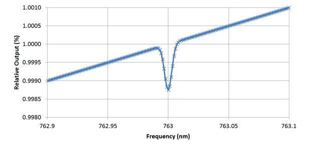
Figure 5. Typical Molecular Oxygen Absorption Line at STP
(50 mm path length)
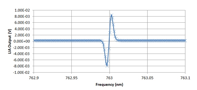
Figure 6. First Derivative of Figure 5 Using Finite Differences.
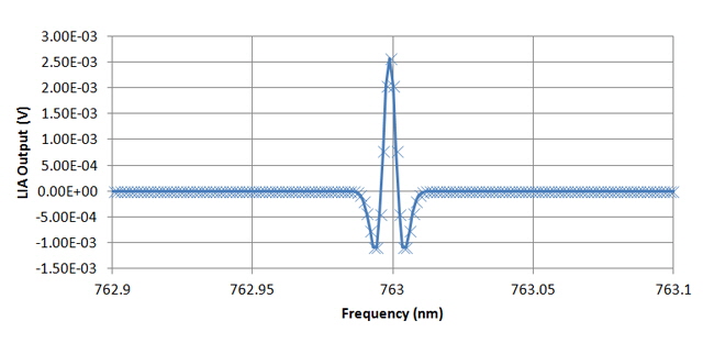
Figure 7. Second Derivative of Figure 5 Using Finite Differences
(Note the slight peak offset from 760 nm due to Excel sampling intervals)
Just for interest I have also simulated the first and second derivatives using sinusoidal modulation. The modulation depth is 20 uA ppk at the laser which is approximately 13 times as large as the digital scheme (1.85 uA).
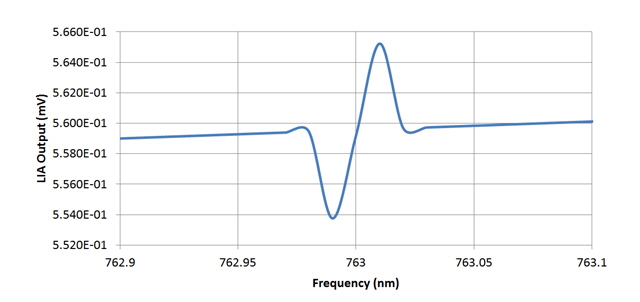
Figure 8. First Derivative of Figure 5 Using Sinusoidal Modulation
(compare with Figure 6 above and note change in vertical scale)
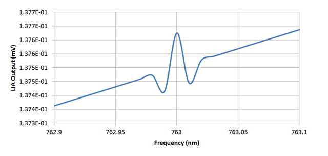
Figure 9. Second Derivative of Figure 5 Using Sinusoidal Modulation
(compare with Figure 7 above and note change in vertical scale
The resulting sinusoidal modulation spectra has a much lower amplitude than the digital scheme and although the base line is linear, it is not flat. You can also see some peak broadening. I haven’t figured out what is causing the base line issue, but the amplitude and broadening are a direct consequence of the depth of the sinusoidal modulation.
As a result of the Excel analysis (see Figure 7) I need a low pass filter with a gain of about 500 to follow the LIA. We are only interested in the DC content of the LIA output. While we ideally want zero input offset voltage the more important parameter is input offset voltage drift. The gain is considered in more detail further down this page.
I have a preliminary design using a fourth order Butterworth active filter which simulates well. I hope to be prototyping this in the next few days. The schematic will wait until it has been bench tested.
Absorption and the Beer Lambert Law
Let’s assume for the moment that we can actually achieve the spectra measurements of the differentials shown above. A very good question to be asking at this time is what is the relationship of these curves to the oxygen concentration?
We can intuitively expect that as the absorption path length increases the light will interact with more oxygen molecules so the absorption will increase and the signal level will drop. The same expectation will hold for increased oxygen concentration.
A fundamental relationship between light transmission at a particular frequency and incident intensity through an absorbing media is the Beer Lambert Law.
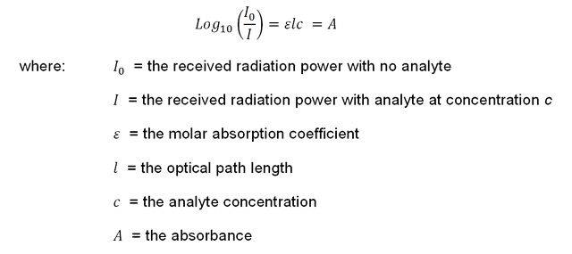
I have deliberately neglected stating units because A is unit-less and the units of E, l and c are not particularly important, so long as they are consistent.
For now we will assume that the analyte is at Standard Temperature and Pressure (STP) and only the oxygen concentration changes.
Also assume for the moment that I0 == 1 (the double equals signs mean exactly) and that E l is a constant, k.
We know that:
for c = 0, I = I0, and A = 0.
the oxygen concentration of air is 20.094%, and
from other described experiments at STP and I0 = 1, I is about 0.99875.
We can re-arrange the Beer Lambert Law to calculate the constant, k, as:
So we can now calculate the expected intensity of received radiation for a given molecular concentration, c. While this expression is clearly not linear, in our range of interest with concentration, c, ranging from 0 to 100% it is very nearly so. If we look at Taylor’s expansion:
we can see that the second term is -0.0062 for c = 100% while the third term is about 20E-6. Subsequent terms alternate in sign and get progressively smaller (this sequence does converge). This means that over our concentration range of interest a linear approximation will be within 0.002% of the exponential.
If we plot I as a function of c over the range 0 to 100% we can see that our linear assumption holds.
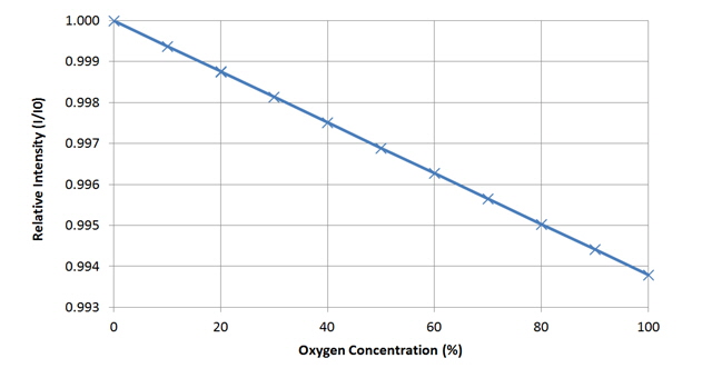
Figure 10. Relationship Between Oxygen Concentration and Relative Intensity
Okay, but we still haven’t answered the question about the relationship between oxygen concentration and our differential and double differentials of the absorption lines? We could figure this out explicitly but I have simply used my Excel simulation to graph these:
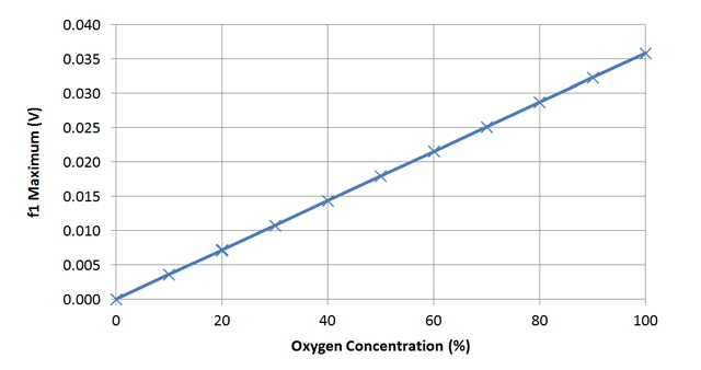
Figure 11. Relationship Between Oxygen Concentration and First Derivative Maximum
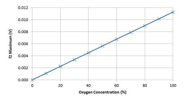
Figure 12. Relationship Between Oxygen Concentration and Second Derivative Maximum
So for our purposes the differentials will have a linear relationship with molecular oxygen concentration. Further, subject to noise, we should readily be able to resolve 1% molecular oxygen concentration at STP.
Note. The use of percentage oxygen is relative to STP. Thus 100% corresponds with pure oxygen at STP, but if we double the pressure then we double the number of gas molecules that interact with the laser. I have not yet considered the effects of increasing pressure but the absorption lines will broaden and intensify.
I have received some useful advice in the past couple of days from my laser manufacturer. They have suggested that temperature stability might be an issue and cautioned that the VCSEL lasers are extremely sensitive to Electrical Static Discharge (ESD). I will comment briefly on each of these issues.
Temperature Stability
The VCEL lasers are tunable by varying the current and the operating temperature. The temperature dependance is about 0.06 nm/K and many devices are fitted with TEC coolers for slow tuning and stability. I figure that there are sufficient oxygen absorption lines in the 783 nm band that the actual operating temperature shouldn’t be too much of a problem provided it remains relatively stable. Stability is easily achieved through thermal mass and air current shielding. Further, TEC’s are relatively inefficient devices. It might be easier to heat the laser than to cool it should thermal stability be a significant issue.
ESD
Now days most semiconductors have all manner of ESD protection on connections to the real world and you would struggle to damage them with static without doing something exceptionally stupid (or thoughtless). But there was a time when MOS and CMOS integrated circuits were not protected from static discharge and if you looked at them the wrong way they would die. This death was insidious - no bang or smoke and not always instantaneous. I recall component level servicing of MOS memory cards where, on analysis, it was figured that the damage had been caused months earlier by inappropriate handling. In those days static handing precautions were mandatory and failure to follow company procedures was a dismissal offence. However the rules aren’t that difficult - just a little time consuming.
Avoid creating static charge through sensible (non-synthetic) clothes and shoe-soles.
Before handing cards or components you, the card/component, and the equipment/card were placed at the same potential through wrist straps, floor and bench mats, and a servicing ground point (usually attached to the machine chassis or Earth).
Cards were handled at the edges and service handles. Components were handled with appropriate grounded conductive tools that avoided contact with leads. Soldering and rework stations were grounded, including the active heating element.
All components and cards were stored in antistatic bags or conductive tubes irrespective of their understood susceptibility to static.
Components and assemblies that have the potential to store or retain residual charge (capacitors in particular) were discharged, usually through the conductive bench mat, before being placed in circuit.
When fabricating stuff by hand the semiconductors went in last and the first pins to be connected were ground, Vdd and Vss (in that order).
Now days many of these precautions seem to have been dispensed with. I still cringe when integrated circuits arrive plugged into blocks of polystyrene and when components arrive in plain plastic bags closed with adhesive tape. While I haven’t experienced a static failure in years I will be reverting to my old school rules before handling my new lasers.
Post LIA Filter and Amplifier
Our next challenge is determine how much gain we need. We anticipate a 3.5 mV second differential peak to peak voltage (see Figure 7). Our ADC reference voltage will be around 2.5 V and we will allow 25% of head room. So our overall gain needs to be about 500. The LIA contributes a gain of 2 and my low pass filter will have a gain of about 2.6 (subject to damping). So we need an additional gain stage with a gain of about 100.
I have prototyped my post LIA filter and Amplifier. The assembly works well but I am experiencing some problems with low frequency noise.
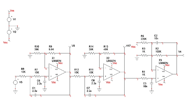
Figure 13. Low Pass Filter and Amplifier
The first two op amps form a fourth order low pass Butterworth filter with a gain of about 2.6 and a cut off frequency of less than 10 Hz. The final op amp is a DC amplifier with a gain of about 100 with R5 (adjustable) providing offset. The LIA is configured to provide an additional gain of 2.
I will need to select precision op amps for this stage otherwise input offset offset will entirely mask the small DC signal that we are interested in. In prototyping this circuit I have used LMC6482 op amps with a typical input offset voltage of 110 uV. If we assume cumulative worst case propagation through the DC amplification chain then we can expect up to 40 mV of offset at the output. The prototype actually performs remarkably well with a measured offset at the output of 22 mV (input grounded).
The most significant issue with my test circuit is low frequency noise. I have established that much of this emanates from:
my bread-board layout,
my lack of appropriately sized capacitors for the PIN diode servo (above) and the filter,
poor power supply decoupling,
microphonics,
a lack of EMI shielding, and
induced mains noise.
In order to make progress I will soon have to abandon the breadboards and revert to fully shielded printed circuit layouts with sensible ground planes, point grounding and independent fully decoupled power supplies.
28 October 2014 and I have some stability issues with my servo (Figure 3). While the prototype works just fine for small signals (say +/- 20 mV) there is a significant amount of 50 Hz coupling with relatively large signals (say +/- 200 mV) and transient instability. On reflection I can see a number of areas where the design could be improved. The cut off frequency of the low pass filter that proceeds the servo (integrator) is too high. The drive for the current feedback transistor, Q1, is not optimized for the expected dynamic range, and Q2 (the common base amplifier) is operating with the collector at the base potential. I am working on an improved implementation.
The new servo circuit is has been constructed and built and the problems with large signals, transients and 50 Hz noise have gone while retaining small signal performance. See Figure 14.
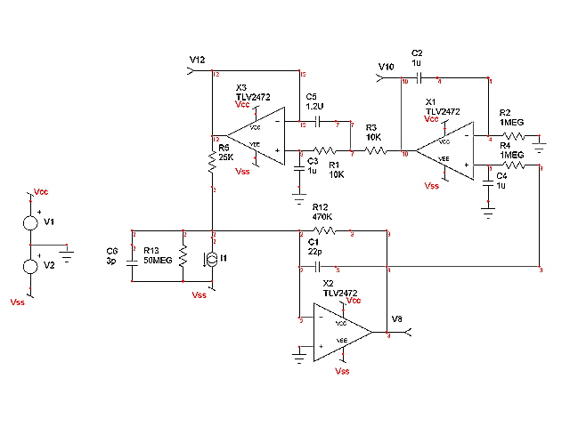
Figure 14. Improved PIN Diode Amplifier and Servo
In redesigning this circuit I have spent some time looking at the stability criteria using Nyquist diagrams and Bode plots. The open and closed loop transfer function mathematics are starting to get complicated so I thought I would use circuit simulation techniques for investigating stability. However this requires all manner of artefacts to force the circuit into a valid small signal mode where upon my simulator ’gets lost’ looking at the internal structure of the op amp macro models. I figure I will need to simplify my model to complete this analysis.
You will see that I have removed the common base stage from the amplifier entirely. The original reason for this stage was to improve the transient response of the PIN photodiode, but my new diodes have minimal capacitance which is further reduced by the increased negative bias obtained without the transistor. The only reason for adding an initial gain stage will be in seeking to improve the signal to noise ratio but for now this isn’t a problem.
The circuit simulates just fine. The transconductance gain has been increased to 470,000 and the LIA second derivative is producing a maximum of just under 6 mV (cf 2.5 mV in Figure 7).
For the record Figure 15 shows the current breadboard prototype and Figure 16 shows the output of the circuit with adjusted LED modulation to better simulate the performance of my lasers. You will see that there are a few red bead Tantalum capacitors sprinkled about the board for power supply decoupling.
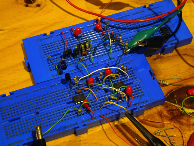
Figure 15. Prototype Laser Drive and PIN Diode Amplifier and Servo

Figure 16. Prototype Large Signal Performance
Vert. 0.35 V ppk. Horz. 1 ms/Div
Figure 16 shows the large signal performance. The signal is symmetrical about ground with output rise and fall times of about 25 us between 10% and 90%. There is an exponential component to (what should be) the flat voltage maximums and minimums. I figure this is due in part to my slow IR PIN photodiode and in part due to my lack of appropriately rated capacitors in the prototype (as mentioned earlier). While these will have virtually no influence on the filtered RMS LIA output, I expect significant improvements in the final implementation.
Cell Design
To date my design has been based on the anticipated output from a 50 mm long sensing path at STP as shown in Figure 5. I figure that I can reasonably increase this to about 250 mm without ending up with an ungainly cell. By using optical techniques such as White or Herriot cells we can increase the optical path length using mirrors which results in increased molecular interaction with the sensing beam and greater attenuation in an absorption band. The trade off is cost and ease of alignment. I have an idea for a helical multi-reflection cell based on a simple cylinder that might significantly increase the sensing path length while maintaining relatively low cost, ease of alignment (by utilising beam-width), and providing a compact design. Like so many design issues there is a compromise in this case between reflection losses, beam width and scattering. Machining a cylinder and polishing it should be relatively easy. Providing a highly reflective corrosion-resistant coating is also relatively straight forward. The only issue I anticipate is machining the input and output ports for accurately mounting the lasers and the diodes.
New Capacitors
My new capacitors have arrived and been installed in the breadboard prototype, still with the LED as opposed to the laser. While the circuit transient response is still slow (entirely due to the LED and photodiode speed) there is now no discernible droop, and the servo action that removes the DC component of the signal is stable and functional across all anticipated operating conditions.
With an LED drive of 2 mA DC with 180 uA 1 kHz square wave modulation the amplifier is producing 400 mV ppk output. In the final application we can expect 80 mV ppk from the intended modulation with a differential signal of interest of about 1 mV.
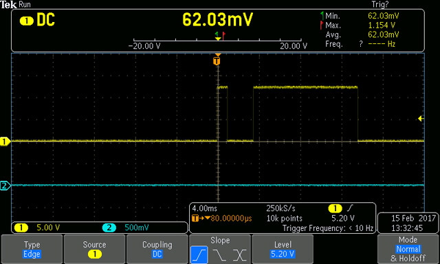
Figure 17. Amplifier Response at 1 kHz
(Blue Trace: 180 uA LED Modulation. Yellow Trace: 400 mV ppk Amplifier Output)
More to follow...
|