|
29 November 2013 and I dusted of my welder this afternoon to make a few thermocouples and welded wire connections for my reflow oven. When I say dusted off that is exactly what I mean. The welder has been sitting idle for months and, as I still haven’t finished the case, it was coated in dust. With a vacuum cleaner and a paint brush I set about cleaning everything, filed the electrodes back to clean copper with nice rounded points and re-bolted the leads to the welder.
With power applied there was no LCD display? A quick check and I found that I had dislodged the power supply plug to the MCU board with the vacuum cleaner. In any future construction I will improve these connectors. With power re-applied I got an error associated with the foot-switch which had become partially unplugged. Excellent!, the software is advising me that I am stupid (and I wrote it so I only have myself to blame on either count). With the foot-switch connection remade every thing appeared to spring back to life.
The intended welds are relatively delicate copper to tinned copper so I set the weld voltage down to 13.5 Volts with a 1 ms first pulse, a 1 ms dwell and a 20 ms second pulse and set about welding a test piece. The first test weld blew the wires to bits. That’s not good (but not totally unexpected).
I reduced the second weld pulse to 9 ms and completed a second weld. The wire didn’t vaporize entirely but there was lots of black weld flash (oxidized copper), one of the electrodes had welded to the wire and I still didn’t have an effective weld.
I reduced the weld voltage to 10.5 Volts, made up another test piece and completed a third weld. The wire only partially vaporized this time with a reasonable weld on the remnants. Hang on a minute. Something appears to be amiss with the LCD display? The capacitor voltage measurement is changing so rapidly between 10.5 and 10.6 that the last digit is a blur between 5 and 6.
I reduced the weld voltage to 9.5 Volts. The LCD display weld voltage was now rapidly fluctuating between 9.5 and 9.4 volts. Before I could make the weld there was an over-temperature alarm from TC2 (charge-discharge heat sink) so I turned the welder off, un-plugged it, and set about using my finger to test the temperatures of the heat sinks.
The charge-discharge heat sink was unduly warm (about 50°C which corresponds with the over -temperature alarm). The heat appeared to be concentrated on the upper half of the heat sink. Nothing else seemed to be unduly warm.
When I put the welder away all those months ago it was working perfectly so what could have changed?
My immediate thought was that one (or more) of the main discharge capacitors has gone leaky. This would account for the charge board heat sink getting hot and the rapidly fluctuating capacitor voltage.
I set about doing some more tests. The first test was a range of bridging wire discharges at constant voltage. Everything appeared to be working fine for the 30 minute duration of the test. The charge-discharge heat sink got warm but there was no over-temperature alarm for the duration of the test.
Next I set the capacitor voltage up to 18 Volts and left the machine on for an hour, checking the temperatures every now and again. The capacitors stayed rock solid at 18 Volts and the charge-discharge heat sink was stone cold. At the end of the test I set the capacitor voltage down but it wouldn’t move. It drifted down slowly at about 0.1 Volts every 10 seconds of so.
The main capacitors are clearly holding their charge and there is definitely something amiss with the discharge board.

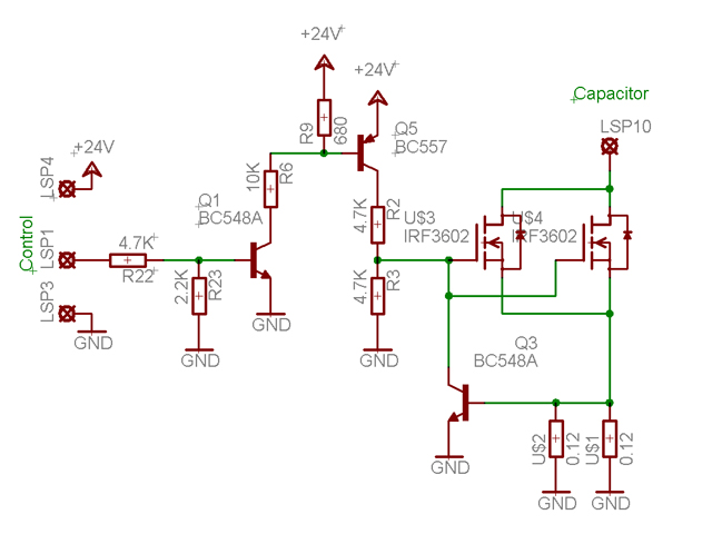
Figure 1. Existing Discharge Board Schematic
I removed the charge-discharge assembly from the welder case. One of the discharge MOSFETs is toast with a short circuit between all electrodes. The current sensing resistors (U$1 and U$2) have failed open circuit, as has the current sensing transistor (Q3).
So what has occurred here (and why)? While the discharge MOSFETs (IRFP4368) are usually operated in pulsed duty they are not appropriately rated for continuous DC currents in excess of 6 Amps with Vds > 10 Volts. As a consequence of continuous operation one of the MOSFETs fused and the current sensing resistors (rated at 5 W) burnt out open circuit. With the resistors open circuit the current sensing transistor also failed. The first failed MOSFET protected the second by putting a short across it. The over-temperature alarm clearly worked, but too late to save the discharge board. This reminds me of a fundamental design rule - semiconductors will always fail to protect their thermal protection!
The discrete logic switch at the front end of the discharge board appears to be fully serviceable so, although I know what has been damaged, I still don’t know what was causing the discharge board turning on when it should have been off.
As a consequence of this failure I need to change the rating of the discharge MOSFETs and repair the discharge board. It won’t be too long before I am back making welds.
I have also rechecked the charge circuit MOSFET (FQA36P15) specifications. They are well within the rated safe operating curve for DC (continuous) charging currents and voltages so I don’t anticipate any problems from this quarter in the future.
As an aside a number of folk have requested complete schematics and board layouts for my welder. I am reluctant to provide these as the design remains work in progress. This current issue (although not yet resolved) has resulted in three implemented design improvements, and a fourth (not incorporated as it requires a new PCB).
I am waiting on the delivery of the new discharge board MOSFETs... The new MOSFETs have arrived and I have reassembled the circuit. Rather than plugging it straight back in to the welder I set about doing some further bench tests to confirm operation.
I started by measuring the MOSFET’s gate voltage. Initially it was switching fine but then it inexplicably started to turn on with no input drive. The collector of the input transistor (Q1, a BC547B) was drifting down yet the base was driven hard off. The input transistor has gone leaky from the collector to the emitter. I replaced the transistor and everything is working fine again. This is entirely consistent with the original failure mode so I suspect that I have found the fault.
The voltage rating (45 V VCEO) and the maximum power dissipation (500 mW) of the input transistor significantly exceeds operating conditions in any mode. Further, the transistor is mounted well away from anything hot so I figure there is no specific cause for this failure - it just happened.
As a final check I have quickly recalculated the current fold-back limit at 13.7 A at 20°C dropping to about 9 A at 100°C. These results were confirmed by simulation. At these extremes the current sensing resistors are dissipating 4.7 W dropping to about 2.8 W. Given that the charge and discharge boards normally operate in pulsed duty everything should be fine.
The welder has been reassembled and appears to be working again. Now I need to get on and make those welds for finishing off my reflow oven. And while I’m about it I should complete the welder case and improve some of the board interconnects!
Oops, we still have a problem!
After about 30 welds another problem has appeared. When the capacitor voltage is turned down the main power supply is occasionally being pulled down causing a power supply reset. Back on the test bench I can see that the cause is an oscillation on the discharge board. Nothing has been damaged but I am struggling to understand what is happening because it is fast and intermittent.
I suspect that the problem is due to parasitic oscillation which is a recognized problem when power MOSFETs are operating in parallel. There may also be an issue with mismatched MOSFET turn on voltage, and I have looked at the software and I can see a potential problem here too. The oscillation is relatively fast (>20 MHz) so this isn’t a thermal issue.
With either MOSFET removed the discharge circuit is operating perfectly. With both MOSFETs in circuit either a reduction in switching speed and/or a reduction in discharge current also fixes the problem.
I tested each MOSFET individually and there is an 0.1 V difference in turn on voltage (but otherwise they are operating just fine all the way up to 20 A Ids - the limit of my test power supply).
Interestingly these particular MOSFETs are not demonstrating the expected thermal self-balancing. The theory is that when a MOSFET gets hot Vgs for a given drain current decreases, but this is more than offset by the increase in channel resistance (Rdson) and the reduction in gain (Beta). However in my DC tests the drain current increased as the device got hot, despite having a fixed gate voltage.
There are several solutions to the oscillation problem. The first is to improve the matching of the MOSFETs. The second is to incorporate a ferrite bead and some resistance in each gate drive. The third is to provide separate gate drives.
In the longer term I will apply the third solution as this will improve current balance, will not reduce switching speed, and will allow the use of mismatched MOSFETs. In the interim I have fitted a ferrite bead and a 100 Ohm resistor as close as possible to each MOSFET’s gate using the circuit at Figure 1 (above).
With the discharge board back on the test bench it is sinking 12.6 Amps beautifully with no sign of instability running from ambient temperature to as hot as hell (no forced air cooling). This confirms that the most recent issue was the parasitic oscillation caused by the change in MOSFETs.
The charge/discharge assembly has been fitted back in the welder and I have completed around 100 discharges and charges over a range of capacitor set voltages just as fast as the recharge and adjustments would allow. The heat sink is getting warm (but not hot) and everything is stable.
As an aside I need to replace the temperature sensors and improve their mounting. All of the disassembly ad reassembly has caused their leads to snap off right at the TO92 packages. I think I have some spare LM335’s in a box somewhere.
On the software, the problem that I have identified is to do with the accuracy of ADC readings when changing voltage references or channels. The Atmel data sheet talks specifically about this issue. In the main command loop the ADC is busy measuring all sorts of stuff (voltages and temperatures). Under some circumstances this could be resulting in charge/discharge cycles when they are not actually required or incorrect temperature readings. The solution is to either time out one ADC cycle after any such change, or discard the first ADC reading.
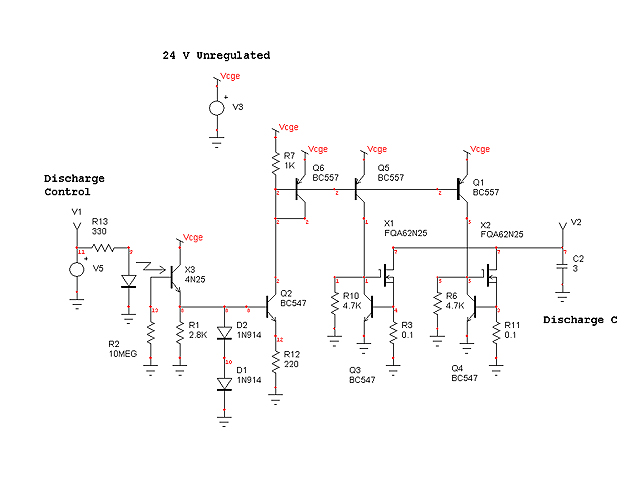
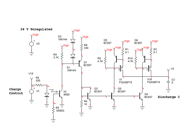
I have redesigned and simulated the charge and discharge boards with separate gate drives as shown in Figures 2 and 3. They require just a few additional low cost components over the earlier designs (at Figure 1). The new charge and discharge circuits are essentially identical in function. Working from left to right: the input is an opto-isolator which switches a 2 mA constant current source. The individual MOSFET gate drives are provided by 3 current mirrors. The maximum gate voltage is established by the 4.7 K resistors at about 10 V. Current regulation and thermal fold-back are provided by the transistors connected between the MOSFET gate and the source. These should be thermally coupled to the MOSFETs or alternatively the 0.1 Ohm source resistors. They provide about a 40% reduction in charge/discharge current for a 130°C temperature rise.

Figure 2. Modified Discharge Board Schematic

Figure 3. Modified Charge Board Schematic
The refinements are:
the change in MOSFET specification to ensure safe DC operating levels.
the input from the processor board is now optically isolated. While this isn’t essential it provides a level of protection to the processor board in the event of a complete melt down, and makes for a more versatile circuit.
The drive transistors now operate as non-saturating switched constant current sources. This improves their switching speed and provides a higher load impedance at the MOSFET gates.
The MOSFET drives are separate, preventing parasitic oscillation, ensuring current balance, permitting gross mismatch of Vgson, and improving the switch off speed by a factor of two.
The MOSFETs are now mounted directly on the heat sink with no mica insulation. This improves heat flow between the MOSFETs and the heat sink which will result in lower temperatures.
Okay, on with my welds. Thank you Santa, for providing me with this improvement opportunity for Christmas!
It’s been some time since I have had to use my dual pulse CD welder but I have some NiCad battery packs that need rebuilding for DeWalt, Black and Decker, and Hitachi hand drills. The replacement batteries and a bunch of pure nickel connection strips are on order. A replacement battery pack for the DeWalt will cost about $200 including freight. The parts for all three packs will cost less than this, and two of these packs are no longer available. In a world of throw away electronics I also considered replacing the drills but that would be even more expensive. I’ll be reporting on this rebuild once the new parts arrive.
Click here to navigate to the next welder page, Weld Head.
|