|
Applying dry film resists and solder mask requires a robust heated laminator. Sure, you can do this with a clothing iron at a pinch for small boards but you’ll struggle for a consist application.
I started by purchasing a low cost home and office heated laminator which I intended to hack until fit for purpose. After some experimentation I have concluded that a low cost two roller laminator will not do for this application because there is no heating control and most importantly, the maximum stock thickness is inadequate for circuit boards. These devices also seem to have a consistently poor build quality. The amount of effort required to make this work will be excessive with no guarantee of success.
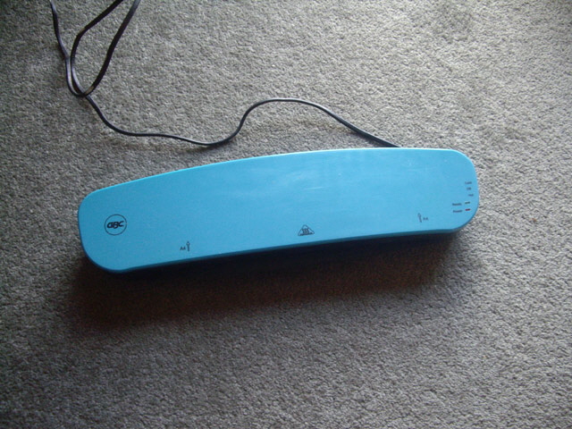
Figure 1. Cheap Nasty Laminator
(Won’t pass a 1.6 mm thick board.)
So I went looking for a moderately priced robust six roller laminator with temperature and speed control, that will handle at least 2 mm thick stock. While an A4 machine would fit the bill I ended up selecting an HC 3306C direct from the manufacturer in China. The machine arrived securely packaged in a foam plastic carrier in a wooden crate.
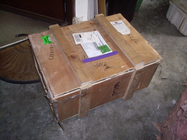
Figure 2. New Laminator Crate
It sure is robust and heavy. The manual isn’t great (Google translation?) and there was some minor cosmetic coating damage on the rear panel. A few of the decals aren’t quite up to the rest of build quality, but the machine heats, has adjustable speed, and passes a 1.6 mm thick board with ease. The temperature controller doesn’t appear to be PID as 30°C thermal overshoot was observed during the initial heating cycle, however it eventually settles down. There is a slight hunting noise on the roller drive train suggesting that something isn’t concentric or is otherwise out of alignment but this is minor and don’t intend to pull the machine to bits just now.

Figure 3. 6 Roll Temperature and Feed-Rate Adjustable Laminator
With a fit for purpose laminator I needs some dry film resists. I ordered some resist films from ebay. For just a few dollars they were cheaper than a single pre-sensitized double-sided (8.0” x 4.5”) FR4 board for 1.5 square meters of coverage.
The dry film resist and solder mask have arrived but I’m busy working on some of the other aspects of the new process for now including Through Hole Plating. The film will be left in its light proof packaging for a few weeks until I come back to my dry film experiments.
Time for my first dry film exposure using an 0.5 W 405 nm Laser.
First focus the laser at a low power setting onto a piece of black anodized aluminium for minimum spot size.
Clean the PCB copper with abrasive pad and dry.
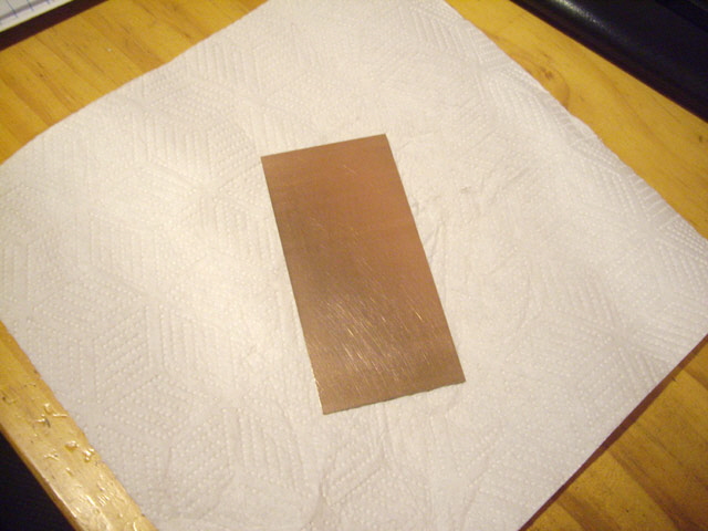
Figure 4. Clean Copper
Cut film and separate non-glossy backing on the concave curled side using adhesive tape.
Apply the film curled side down to the clean copper and laminate at 110°C with speed setting 5. I used four passes. Some bubbles were apparent under the film. This was my fault entirely. I should have smoothed out the film before putting it through the laminator. Now let the board cool for a few minutes.
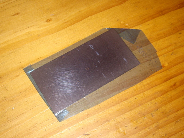
Figure 5. First Attempt at Laminating
(Not great - more practise required.)
The pattern for the exposure was my standard test pattern @StandardTest.nc with a traverse rate set at F1000 and a laser power of S20. Due to a problem with the setting of my Trinamic stepper motor micro-stepping the test pattern was half size and the traverse rate was actually 500 mm/min.
The exposure time for the full pattern was 11:38. The board was clearly over exposed.

Figures 6. First Laser Exposure. Half Sized and Clearly Over-Exposed
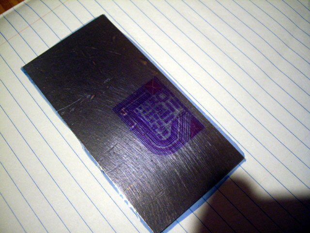
Figure 7. First Laser Exposure. This Isn’t Looking Good
The board was developed in in 0.85% wt/wt Sodium Bicarbonate (8.5 g /litre) at 30°C although literature suggests that up to 30 g/litre is also effective at room temperature.
The result was interesting. The developed board was grossly over-exposed in some areas with the film being burnt exposing the copper beneath. The exposure is blurred between tracks and around the test pattern perimeter from excessive laser fringing. The actual track, pad and text detail is nice and clean, right down to 0.5 mm high text. The smallest pads on the test board (inadvertently printed at half scale) are an LGA12 package with and actual exposed size of just 0.125 x 0.1375 mm, separated by 0.1125 mm spaces. The laser central spot size is approximately 0.15 mm in diameter.
The laminate bubbles failed during development. More laminating practise is required here.
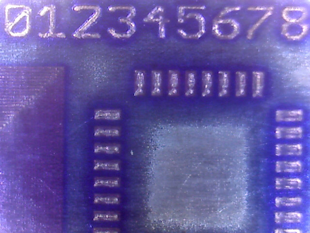
Figure 8. Over Exposed and Burnt to Copper
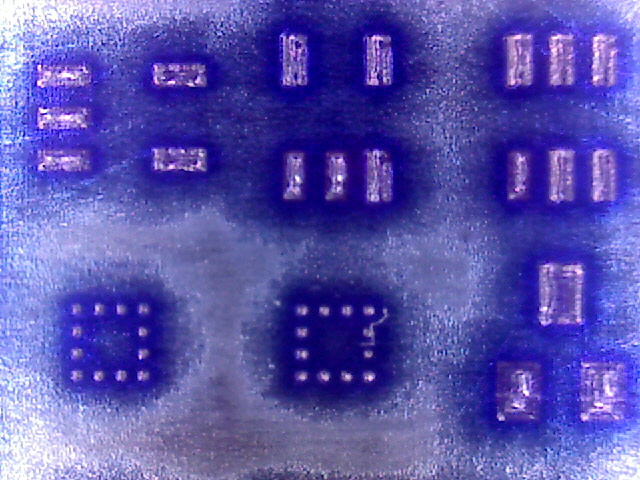
Figure 9. Half Scale LGA12 Package Over Exposed
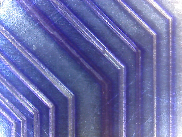
Figure 10. Tracks Burnt Through and Over Exposed Between
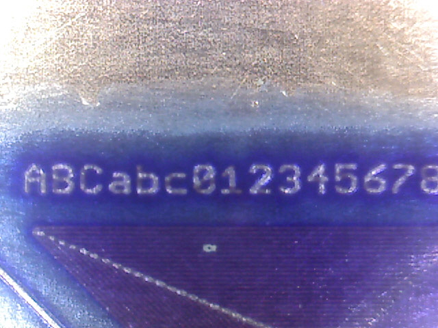
Figure 11. Text Actual Height 0.5 mm and Solid Fill
I cleaned the board with back to bare copper with Sodium Hydroxide solution (20 g/litre) and tried again. I reduced the laminator speed from 5 to 3 and the laser exposure from S20 to S10. The dry film adhesion was much improved, but I’m still burning the film and over-exposing off the tracks.
Before I consume more dry film I need to take a look at the laser focal spot and try and sort out the fringing. My laser diode has a rectangular edge emitter with a Gaussian (as opposed to top hat) profile and is highly divergent, and polarized. I suspect that this particular laser module is multi-mode. As a consequence the source isn’t circular, has a relatively wide bandwidth, and astigmatism. So isn’t at all surprising that there is significant fringing.
A photo of the laser spot at distance of 1.5 m shows exactly what we are trying to focus. It also identifies that we have some dust and maybe a fibre on the optics. The outer limiting ring is simply the diameter of the lens barrel. On inspection the optics are pretty poor. There is a compression spring that holds the focusing lens in place which adds to light scatter, and the inside of the lens housing is bare brass. After a few adjustments the focusing lens thread becomes very sloppy as the two bands of thread filler paste wear.

Figure 12. Laser Spot at 1.5 m
The easiest solution is to place an orifice after the lens to limit the beam to an even illuminated circle, which will also reduce the beam power. But as the orifice size reduces, the fringing increases. At S100 you can clearly see a halo fringe that is resulting in off-track exposure. And the actual extent of the halo sufficient to expose the dry film can’t be seen by eye.
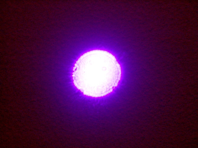
Figure 13. Beam at 1.5 m At S100 with 1 mm Orifice on Focus Lens
While we can’t see 405 nm light very well, we can use a collimated green laser (which is hopeless for dry film exposure but highly visible to the eye) shone through a 1 mm orifice projected a distance of about 6.8 m to make a diffraction pattern visible.
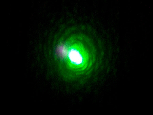
Figure 14. Green Laser Diffraction Through a 1 mm Orifice
I also experimented with a polarizer using an old pair of 3D glasses. The beam is highly linearly polarized but using a plastic film polarizer this isn’t much good for power control because even at low laser output power the laser burnt the polarizer. Oops!

Figure 15. Polarizer Experiment Maximum Transmission

Figure 16. Polarizer Experiment Minimum Transmission
While I was messing about I tried exposing some activated strontium aluminate (glow powder) to the beam. This really charges up fast with the laser and glows brilliantly with the briefest exposure. Interestingly, this also shows the fringing issue, with the fringe being about the width of the central spot on either side.
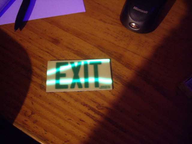
Figure 17. Activated Strontium Aluminate Exposure
So I need to come up with an optical arrangement to reduce the beam power, remove the halo and prevent diffraction. It must not cause spectacular reflections (these are potentially dangerous), must be easy to focus and allow for simple alignment.
I’ve had another thought. Maybe the fringing isn’t a focus problem at all. Perhaps it is ‘halation’. We can reasonably expect the dry film resist and Mylar protective layers to refract and reflect the beam. The bulk of the beam energy is hitting the copper and most of this is reflected (actually absorbed and re-emitted) at all manner of angles. The reflected light then re-reflects off the resist and protective layers forming a halo (the observed fringing).
With my previous pre-sensitized boards there was no outer protective layer and the light source was comparatively weak compared to the laser. Any halo was of insufficient intensity to expose the resist.
I set about completing some further experiments with orifice plates and collimating lenses trying to produce a smaller, lower powered spot without fringing. Messing around on the bench I tried various orifice diameters ranging from ~0.1 mm to 2 mm and a number of lens configurations, but nothing was working very well. A bench test of a pinhole orifice at low power setting (S15) produces what appeared to be a very small spot but the diffraction and halo were appreciable, although really hard to see because the spot is so bright.

Figure 18. Attempts to reduce power and Spot Size
(Note laser module has an adjustable focus lens.)
Midway through my experiments and the laser module output power suddenly decreased. I figure I have damaged the laser, possibly due to overheating as the cooling fan doesn’t operate at reduced S numbers. So I need a new laser. Bugger! I’ll be trying to get a single mode 405 nm device rated at about 100 mW and with improved optics. If necessary I’ll get some laser diodes and build the optics and drive electronics. Unfortunately laser exposure of the dry film is on hold for now, but I can still expose the dry film using my conventional process.
While I’m waiting for my replacement diodes I thought I’d try conventional UV lightbox exposure with the dry film resist. The first issue is making a negative from my antiquated version of CadSoft Eagle. This is necessarily a graphics processing process but it works.
Open the board in Eagle.
Hide layer components that you don’t want to print.
Ratsnest to fill in any solid fill polygons on supply planes.
From the file tab select Export and Image.
Set an appropriate dpi for you printer (2400 works for me).
Select monochome.
Save as a TIF file (although other file formats are available and may be appropriate subject to you image editor).
Now open the file in Adobe Photoshop.
For layers viewed from the top you must flip the image in the horizontal plane to get the toner against the dry film resist.
Apply any necessary scaling to calibrate your printer’s absolute accuracy
Select your printer and set it to the same dpi (2400), set in the Export.
Print onto Mylar film.
I quickly laminated up a test board, set the negative and exposed it for 1:45. I suspect that this is too based on the exposed area colour and the excessive effort required for development. Perhaps 1:20 might be more appropriate? This needs an exposure test strip which I’ll complete tomorrow.
Remove the upper Mylar and develop in 30 g/litre room temperature Sodium Carbonate solution. This took a while (probably slightly over exposed) and in my impatience I used a small brush which caused a couple of the tracks to partially lift. Maybe I should increase the lamination temperature a tad too.
The results are nice with 1 mm high text clearly readable, and 100% track separations including 0.01” (0.254 mm) track clearances. There was some slight rounding of the LGA12 pads, three partially lifted tracks, one missing character and one missing LGA12 pad, all of which are entirely preventable with appropriate laminating, exposure and developing.
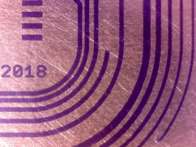
Figure 19. Tracks and Separations at 0.01”
(Light box exposure.)
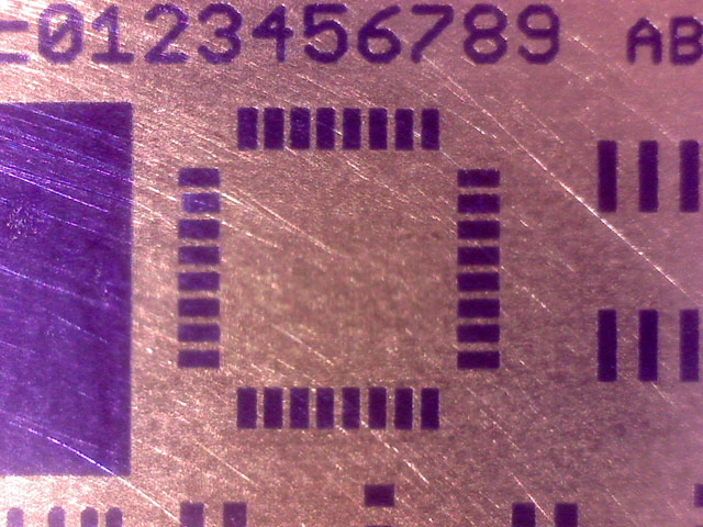
Figure 20. Clean TQFP 32 and SO 16 Packages
(Light box exposure.)
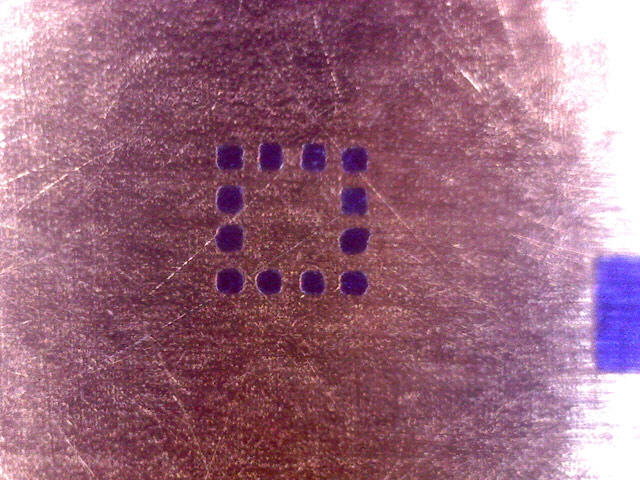
Figure 21. Clean LG12 Package
(Light box exposure.)
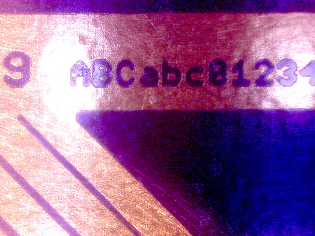
Figure 22. Legible 1 mm High Text
(Light box exposure.)
My direct laser exposure process is going to struggle to compete with my light box unless I can get a clean small circular spot without fringing. In the interim my plated through hole chemicals have arrived so I’ll be experimenting with through-hole drilling on the CNC mill (which I haven’t actually done yet) and trying to get the through hole plating process sorted out.
If I’m going to be using my conventional UV light box then I need to run an exposure test strip to determine optimum exposure time. The dry film is relatively sensitive requiring just 60 seconds exposure compared with 105 seconds for my previous film. Under or over exposure both have disastrous consequences. 105 seconds is way too long and results in light leakage through toner black, and a resist that is difficult to develop. 40 seconds or less and the exposed resist starts to degrade in the developer.

Figure 23. Exposure Test Strip
(20 to 100 seconds left to right.)
I have ordered a new 500 mW laser module because it is fun to burn stuff, but I have also ordered ten 120 mW laser diodes. These should be much better for CNC exposure due to the reduced power and hopefully a smaller emitter. More to follow on this...
I have just received ten SLD3235VF 120 mW 405 nm laser diodes. These operate at maximum duty with a forward voltage of 5 V at 140 mA, with a maximum temperature rating of 80°C.
Driving them from a variable 12 V supply requires a series resistor with a minimum value of:
An appropriate power rating is:
The laser diode will dissipate:
So the laser diode could do with a moderate heat sink. In practice it does run warm (but not hot) in free air at a current of 60 mA.
Best I add a reverse bias diode (1N914 will work just fine) to look after transients and provide protection from inadvertent reverse polarity connection. I’ve increase the resistor to 100 Ohms to ensure that the laser diode is operating at no more than 50% of rated output.
Although this laser has a relatively low output power it is still a Class IV device. Avoid skin exposure anywhere near a focal point (it will still char thin paper at rated output power) and avoid eye exposure to the beam or spectacular reflections. Your blink reflex is not fast enough to protect your vision.
The minimum lasing current is specified as 40 mA but the laser appears to lase right down to 25 mA. The photodiode has a linear measured slope of -0.0268 mA / mW reverse biased from -5 V via a 1 K Ohm resistor (which saturates at 5 mA). Assuming that the data sheet rated 120 mW output is achieved at 140 mA then we can reduce the output power down to just a few milliwatts which should ensure exposed dry film resist without burning.

Figure 24. Measured Laser Output
The beam emission shape is elliptical with a relatively wide divergence so we still need an optical system to achieve a focal spot. With a 14 mm focal length convex lens I get a nice small focal spot, but the fringes still appear to be significant.
By introducing an 0.5 mm pin hole at the focal point (a spatial filter) the fringing is reduced, but alignment is tricky to say the least, and the fringing re-appears at the next lens in the optical path. This leads me to believe that my cheap lenses are contributing to the fringing problem. I suspect that they either don’t have an anti-reflective coating, or it isn’t appropriate for 405 nm. Good biconvex lenses for this wavelength are very expensive (more than $100 each) and sometimes you get what you pay for.
I have an old defunct computer DVD drive (player/recorder) that no longer records and is not worth the effort of repair. I’ve pulled the optics out which includes two beam splitters, a prism, what appears to be a polarizer, and four lenses (all coated), one working laser diode (the read illumination), and a pin diode (the read detector). All have apparent anti-reflective coatings. The fringing certainly reduces with these lenses.
For my crude optical experiments I have been using 3D printed parts as lens holders and barrels. These work well for keeping stuff aligned but plastic does not make an effective heat sink for the laser diode. If I can get the optics to work adequately I’ll make an aluminium housing.
The laser module has been built. It is light and robust with a small circular evenly illuminated focal spot. There is still some flaring evident, but I need to do a test exposure of some dry film to see if this is still a problem.
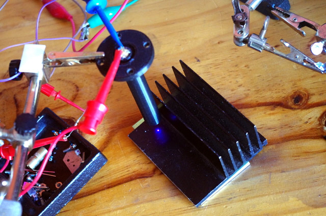
Figure 25. Laser Module Assembled

Figure 26. Laser Module Mounted in CNC Mill
A few design notes (these have a mathematical basis but I won’t be going there just now):
The final focus lens needs to be close to the dry film for smallest spot size. The best I can do at the moment is 15 mm.
The beam, prior to the collimating lens, needs to have a relatively large diameter so we are only focusing the central, evenly illuminated, section.
The optical path should be black to absorb reflections.
Alignment is, as you might expect, important.
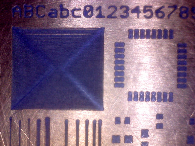
Figure 27. Test Exposure
(The 0.1 mm Spot Size is too small and we still have too much flaring.)
An experiment with my standard test image at a speed of 1000 mm/min and a power level of S100 shows we have a very small focal spot of just 0.1 mm and adequate power for dry film exposure without burning. The focal spot is actually too small and flaring is still a problem, particularly at start and stop points and abrupt changes in direction. The track edges are nice and clean and this is an improvement over the 500 mW laser module but the exposed image is still very poor when compared to my light box. I can increase the diameter of the beam easily but there is no easy fix for the flaring. I figure that I need better optics and I’ll continue to experiment with this.
But in the meantime I’ll proceed with using the light box. exposure which produces consistently great results.
Dry Film Solder Mask
A solder mask isn’t essential for prototypes, but when it comes to ease of soldering fine pitch SMD devices you’ll be saving a lot of effort and potential rework.
I’m using Dynamask 5000 dry film solder mask. This is negative acting, just like the dry film solder resist. The areas of resist exposed to UV light will remain. So we don’t want to expose component pads, test points, or vias.
My first attempt at the process was as follows.
Clean the board, wash it, degrease with acetone, and dry at 120°C for 30 minutes. Drying is really important or the mask won’t adhere. I’ve been using my toaster oven for heating processes but this isn’t a very clever idea. The problem is that this oven is radiant heating as opposed to convection oven. As a consequence the board gets too hot. I’ll need to incorporate a radiation shield between the elements and the board tray in the oven.
In subdued or yellow light cut the dry film to size for both sides. Remove the matt (non-gloss) side with two pieces of adhesive tape and smooth over the board from one edge to remove air bubbles.
Laminate both sides at 65°C with four passes at a speed setting of 3. I seem to have a couple of bubbles so I may need to adjust the temperature, speed and/or pressure here.
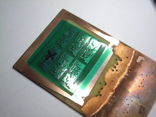
Figure 28. Solder Mask Laminated
Align and fix the artwork, toner side to the copper, with adhesive tape.

Figure 29. Artwork Aligned
Expose the board to UV light for about 60 seconds on each side and let it rest for about 10 minutes.
Remove the glossy protective film with adhesive tape and develop in Sodium Carbonate solution (10 g / litre) at about 35°C.
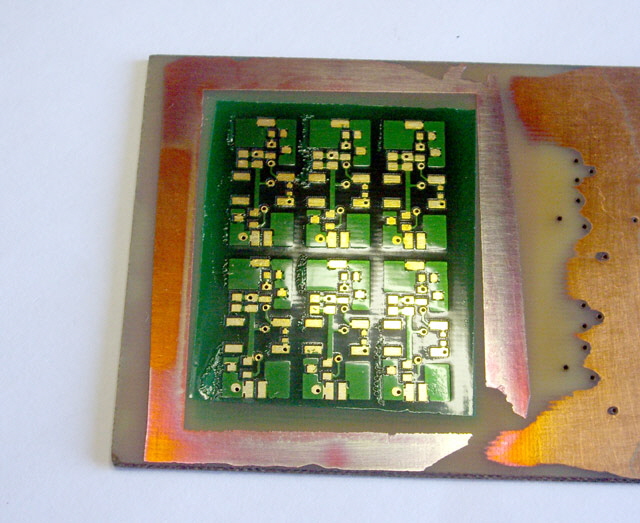
Figure 30. Solder Mask Developed
(I’ve over heated the board during drying.)
The resist layer will be soft just now so avoid touching it. Rinse in water.
Inspect the board for alignment and film adhesion. If you have made an error then the film will soften and eventually strip in Sodium Hydroxide (10 g / litre) at about 35°C. Yes, I made some mistakes.
Cross-link the resist with UV exposure of each side for about 30 minutes. Then thermally cure by convection baking the board for one hour at 150°C and allow to cool. Again, I made a mistake with my radiant heating oven and over-cooked the upper layer of the board. Silly me!
This process almost worked first time for me except for the oven issues, mixing up positive and negative acting again, and in my impatience neglecting to adequately dry the board before laminating the dry film. The second attempt was better but the film adhesion still isn’t perfect. More experimentation is required here.
I’m going to Tin plate this board to make for easy SMD soldering (and I don’t have the equipment for lead free Hot Air Solder Levelling (HASL) finishing. This uses my previous process which works very well using proprietary tin plating crystals.
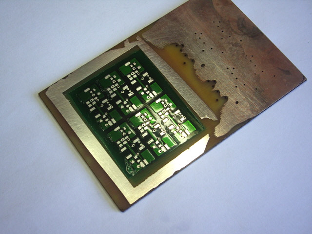
Figure 31. All Done
All that remains to be done is to cut the boards from the panel, assemble and test. Job done!
Well not quite. I’ve been somewhat frustrated by the bubbles that kept appearing when laminating my dry film. Time to take the covers off the laminator and inspect the rollers. The rollers weren’t clean with some dry film stuck to the lead upper roller and some grease spots from the drive gears. The upper rollers are held in place by a latched hinge which allows them to be opened for inspection and cleaning. One of the two latches wasn’t fully engaged so I figure that the roller compression can’ t have been even and sufficient across the board. This probably causing uneven heating of the dry film too. With the rollers cleaned and the latches fully engaged the bubbles have gone away.
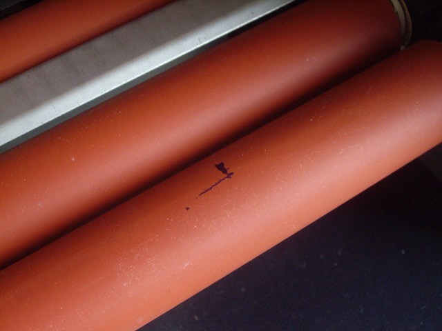
Figure 32. Resist on Lead Roller

Figure 33. Grease on Lead Roller

Figure 34. Frame Latch not Locked
|