|
I’ve got a few lasers here for various legitimate purposes such as pointing at celestial objects in the night sky, presentations, levelling and aligning, distance and angular measurements, gas sensing, smoke density measurement, marking stuff (okay burning), and so on. Most contain a commercial laser diode with at least an element of home construction associated with the final. A few have quite high pulse power at around 27 W but their duty is limited and the driver hardware is critically complicated.
Quite few years back I purchased a 50 mW green DPSS (Diode Pumped Solid State) laser module. I built it into a water proof tubular aluminium case complete with two AA cells for use as a pointer in scuba diving and air. I had reason to try and use it a few weeks back but the collimating lens had changed focus. Unfortunately the brass housing had become corroded over time and in trying to loosen the focusing threads the collimating lens chipped under compression.
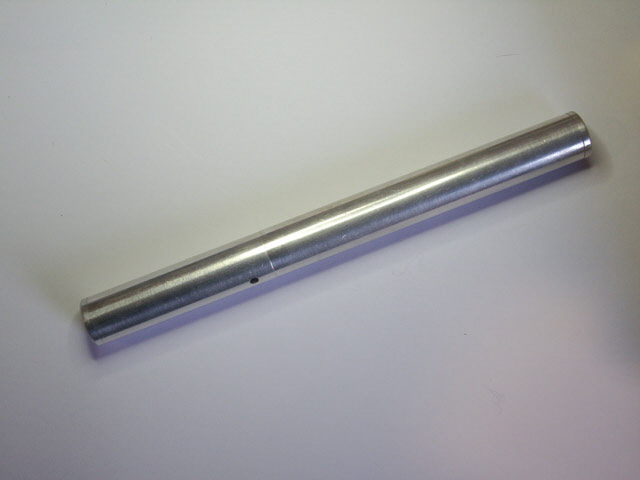
Figure 1. Original Aluminium Housing
After eventually freeing the focus barrel I powered up the laser from my bench supply at 5 Volts. It lased brilliantly for about 5 seconds and died. On inspection the laser photodiode connection has broken internally. This is probably a consequence of a lack of adequate driver board support so that every time the push button was activated it placed stress on the laser diode leads. Without the photodiode current feedback the laser current was excessive (hence the brilliance) until either the laser diode or the Solid State Laser overheated. The laser anode connection also broke right at the case during my inspection measurements. The laser driver board still works fine but the laser is buggered even thought it still draws around 600 mA and glows red.. Resurrecting the module is going to be really tricky. It will be cheaper and easier to get a new laser green DPSSL laser module, adapt the current case to fit it, and add some decent board support. While I’m about it I can increase the laser power rating from 50 to 100 mW.
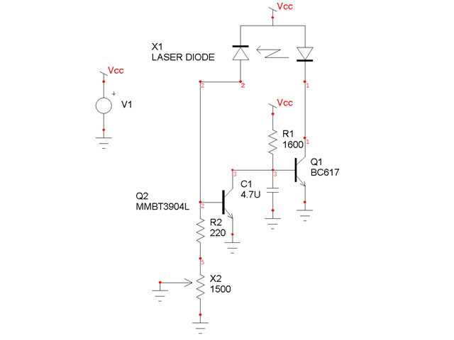
Figure 2. Original Beam Output Regulated Driver

Figure 3. Original DPSSL - No Beam
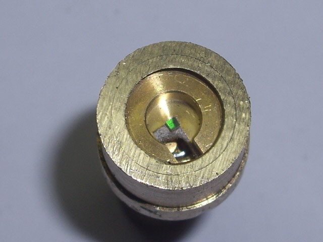
Figure 4. Original Solid State Laser with Diode Pump Below
I ordered five 100 mW modules and they arrived in just a couple of weeks. They have a slightly wider brass barrel for the collimating lens and are about 10 mm shorter than my original module. The driver board, a small adjustable constant current source, appears to be more complex than the original and the actuation switch location has changed by a few millimetres. However the old case can be adapted to fit the new modules.
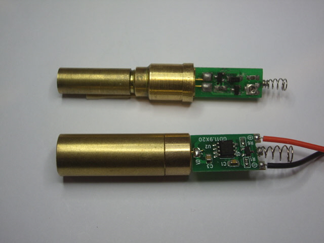
Figure 5. Original (above) and Replacement (below)
First things first. I need to test the new modules using two AA cells (3 Volts). Two of the modules appeared to work fine, with a reasonable beam intensity (just visible in my office with ambient daylight) and circular focal point, but the devices were getting very warm very quickly. A further module had reasonable beam intensity but the focal point was a double circle. The last two modules had abysmal output.
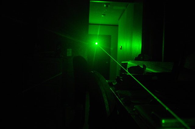
Figure 6. New DPSSL at 500 mA. Nice!
Double A batteries don’t last very long under significant load so I arranged a stepped 4.4, 3.8, 3.2, and 2.7 voltage supply from a 5 volt bench output using four series-connected 1 Amp silicon diodes, a 1 K Ohm quiescent resistor to ground and a 1,000 uF 16 V electrolytic capacitor to ensure the supply voltage remained constant under load.
With an ammeter to measure the module current and a voltmeter across the laser diodes I tweaked the current adjustment potentiometer while observing the beam intensity. When first turned on the beam output is low, but it improves as the module housing warms up (to sensible hand-held warm). At 500 mA the laser output is brilliant, but everything is getting very warm very quickly.
Once warm the optimum module current for beam output appears to be about 350 mA from a 3.2 Volt supply but the beam intensity continues to vary over time. The current regulation appears to be stable. After adjustment to 350 mA all five modules now had adequate beam intensity. The constant current boards are still getting uncomfortably warm after just a minute of operation at 3.2 V, 350 mA. The culprit appears to be the D882 output regulating NPN transistor. I’ll need to have a look at this later.
The voltage across the laser diode is about 1.9 Volts at 350 mA for all of the modules. I figure that this is about right for a DPSSL running at 20% efficiency with an output of 100 mW.
After getting the laser intensity about right I now have two modules with focus issues. I removed the collimating lens barrel, used a fine hair bulb brush on the optical path, and gently wiped the optical surfaces with a clean dry cotton bud. With the lens barrel refitted the modules are now making a nice circular spot (about 4 mm diameter at 3.5 m).

Figure 7. New DPSSL Structure
(Collimating lens removed for cleaning)
Time to try powering the modules from the AA batteries again, but with the instrumentation attached. That’s weird! The current is not regulating to the 350 mA set point and steadily increases to over 500 mA on all modules. The beam looks great but stuff is getting beyond comfortably warm. Power off! This needs to be investigated.
Before proceeding it is worth while noting that DPSS lasers without temperature control can be expected to have variable beam output. This is a direct consequence of changes in the absorption spectra of the solid state laser and the frequency doubling medium due to temperature variations and associated thermal expansion. Cheap DPSSL modules don’t have active temperature control or photodiode beam feedback. They rely on the thermal mass of the laser housing, associated conductive/convective cooling and short duty cycles to keep the laser from getting too hot.
The suppliers instructions for these modules state that they should only be operated for short periods (or words to that effect).
The very next step is to draw out the schematic of the driver board. The circuit is a current regulator. It uses an operational amplifier to compare a set voltage derived from a precision temperature stable IC voltage reference against the voltage developed from the lasing current across an 0.5 Ohm resistor. The op amp provides negative feedback to the base of the output transistor to maintain the lasing current at the set point. The 0.5 Ohm current sensing resistor also provides negative feedback from the emitter to the base.
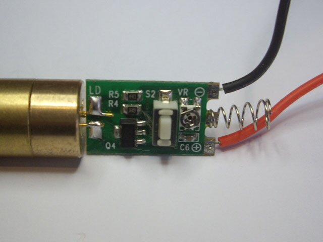
Figure 8. Top of Current Regulator Board
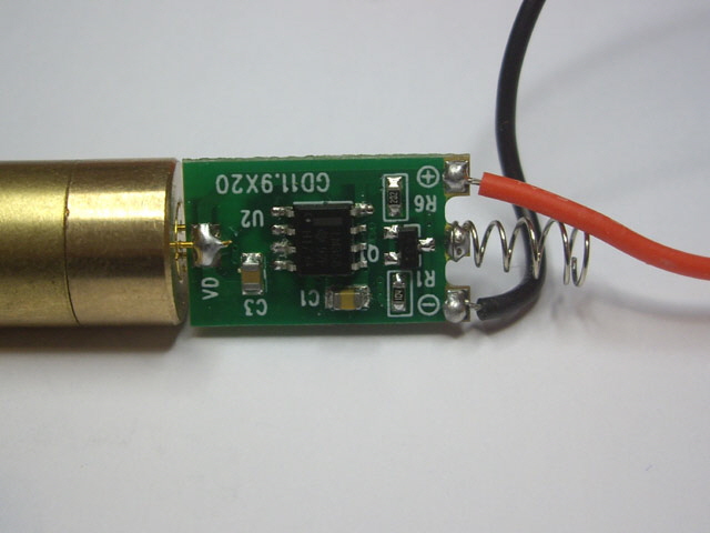
Figure 9. Bottom of Current Regulator Board

Figure 10. Constant Current Schematic
There are a whole heap of problems with the constant current driver design.
The op amp is rated for 3 V minimum operation. Under load the supply voltage from AA cells at the op amp is below 3 V. Op amp functionality is therefore no longer assured, and sure enough current regulation is lost operating below 3 V.
Only one of the two op amps in the LM358 dual package is utilized. The unused op amp has input and output pins floating (not connected). This is poor design practise and can cause all manner of problems including latch-up and oscillation. A dual op amp should be more expensive than a single device package and take up more board space. More bad design.
The output transistor is under-rated with a maximum dissipation of 0.5 W. The transistor power dissipation will be exceeded with supply voltage of about 3.5 V. Operating so close to rated margins is poor design.
The current adjust trim pot is cheap and nasty with no end stops. I just hate these to bits.
The precision reference, a TL431, has a maximum rated output of 2.52 V and a worst case minimum cathode current of 0.7 mA. The cathode current is provided from a 2 K Ohm resistor from the positive supply rail. Hence there can be no surety that the reference will operate correctly with Vcc less than 3.5 V. This aspect of poor design is not hypothetical. With Vcc at 3 Volts the current regulator board stops regulating and the current steadily increases to the limits of the supply. This is laser module death!
The laser diode leads extend beyond their mounting pads and risk shorting to other PCB tracks (insulated only by the solder mask). Tacky design and construction.
The board dimensions are apparent on the silk screen mask: GD11.9X20. Unfortunately the board designers have not made an allowance for Vee notch board separation cut. So the actual board width is 12.10 mm, which is larger than the brass laser module housing. Poor design and construction easily averted with a milling cutter or an allowance.
The driver board is supported by the laser diode pins. So eventually the pins will fail through stress induced by operation of the push button switch (exactly the same failure mode experienced by my previous laser). Perhaps the best solution to this problem is to use epoxy resin to adhere the board to the back of the brass case, reinforcing the laser diode pins and actually improving heat transfer from the laser to the board.
There is no polarity protection for the board. If you connect it the wrong way around the op amp will likely be stuffed due to two internal silicon junctions connection from transistors between the supply rails. This is explained explicitly in the data sheet (and I am not going to try this deliberately to see what happens).
There is no capacitive filtering directly across the op amp supply pins. As a rule of thumb all integrated circuits should be capacitive decoupled close to their power supply pins. Refer to the op amp data sheet. However the supply is decoupled with a small (say 0.1 uF) ceramic capacitor, C6, at the power supply terminals.
There is insufficient copper on the board for effective thermal management. We can use the copper laminate to dissipate heat away from parts that are expected to heat up, while reducing heating of other temperature sensitive components.
There are some aspects of the design that are good.
Track widths are appropriate for current rating and the laser power traces are relatively short and wide (low inductance).
The design does incorporate a soft start feature through the TL431, the associated resistive divider, and the op amp +ve input decoupling capacitor.
The two parallel 1 Ohm 0805 package laser current sense resistors have a combined adequate power rating (0.25 W) good for 0.7 A. While arguably we could use a single 0.5 Ohm 1206 package this component is likely to be significantly more expensive (say a factor of 10) than the smaller 0805 devices.
I think we can do better than this to ensure:
Reverse polarity protection.
Stable operation between at least 2.7 and 5 Volts.
Maybe reduced component count and cost.
Temperature feedback at say 500 mA at 10°C dropping to 300 mA at 40°C.
Better thermal management.
And perhaps a smaller board.
On with the new design.
Let’s start with the TL431 precision reference by replacing it with a JFET constant current source driving a resistor with a parallel capacitor filter. JFET’s have quite a wide range of Vp Idss for a given device type, perhaps varying by a factor of 4. This means that we must incorporate some form of manual current adjustment. Design starts with selection of a JFET with a suitably low Vp max for our 2.7 Volt minimum rail. A BF862 has Vp in the range of -0.3 to -1.2 Volts with a corresponding Idss of 10 to 25 mA. This gives us 1.3 Volts headroom for the reference voltage, laser current monitor, and reverse polarity protection.
A JFET constant current source should have Id << Idss to minimise the effect of parameter variations and to increase the output resistance. If we assume an output current of say 0.5 mA we can calculate Rs at the JFET parameter limits using conventional formulae for Id in the pinch-off (active) region:
Id = Idss (1 – Vgs / Vp)2
The solutions for Rs at the limits of Vp and Idss are 465 and 2,058 Ohms so a 2.5K Ohm potentiometer will ensure adequate adjustment for all JFET parameter variations to provide an adjustable 0.5 mA constant current source that will operate with a supply voltage of no more than 1.2 Volts. Note that 2.5K Ohm trim pots are not a preferred value and we may need to increase this to 5K.Ohms.
JFETs have a particular value of Id that will minimise temperature subject to device specific Vp. However we cannot have both a zero temperature coefficient and some arbitrary constant current (0.5 mA in this design) across the range of JFET parameters. This won’t be critical because I will be applying substantial negative current feedback for temperature rise.
Now let’s reduce the op amp from a 3 V dual device package to a single device with a Vcc min of less than 2.7 V. Note that the input common mode range must include ground, the device should have a single supply, with rail to rail outputs. This automatically fixes the unused device issue.
Let’s go for a MOSFET laser driver as opposed to a power transistor. This has the advantage that it will have a much lower Vgs than a transistors active mode Vce allowing effective regulation at a lower power supply voltage. I have selected a 1.3 W MOSFET which will extend the supply voltage to at least 5 V at 500 mA. The gate control voltage is well within our available supply and op amp capability. The MOSFET is also more efficient than the BJT as there is no base current.
The gain of the op amp and MOSFET is established at 2 A/Volt by the 0.5 Ohm current feedback resistor and negative feedback. While we can calculate this explicitly, a simpler approach is to consider the output MOSFET and 0.5 Ohm resistor as a Source Follower with a gain of 1, and the op amp as an ideal gain block with infinite gain. So:
Again = Vin / Vout = Aforward / (1 + Aforward x Afeedback)
So:
Afeedback ~ infinity / infinity = 1
And the output current is established by the resistor:
We can also use a MOSFET (the same type) as battery polarity protection for the laser module with less than 0.1 V drop at 500 mA. This is a simple circuit but I have added a resistor so we can control the MOSFET with the on off switch. The switch rating can now be reduced as it is no longer switching the laser current.
Heat
Too much heat will shorten the life a laser diode. Most Continuous Wave (CW) 808 nm laser diode pumps are rated at 40°C maximum case temperature (but some have higher ratings).
During my experiments I also qualitatively noted the beam brightness. It actually starts low with the laser module at ambient temperature, increases as the temperature rises and finally begins to decrease as we approach 40°C. Any time that the beam reduces in intensity will cause an increase the heating rate because the lost beam power must be dissipated in the laser diode. This is a potential cause of thermal runaway.
There are a few possible solutions to the heating issue.
Limit use to just a few minutes with an extended off time.
Reduce the laser current (with a reduction in beam output power), perhaps using temperature based negative feedback.
Improve the heat dissipation through fan-forced air cooling and an improved heat sink design – not practical for a hand held laser pointer, although this works under water with the exterior aluminium case acting as a heat sink.
Add forced cooling using a Peltier cooler or similar – not practical for a hand-held laser pointer.
Measuring the brass case temperature is not straight forward. If you apply a point thermocouple with exterior insulation then you are actually changing the conditions which you are trying to measure, and getting good thermal contact with the brass housing is difficult. I completed some rough and ready measurements on three laser modules and the results are at least indicative of case temperature with laser diode current.
At 350 mA from 3.2 V the current laser module brass cases exceed 40°C from an ambient temperature of 17°C within 10 minutes. The diode pump laser case will be hotter than this, but not by much because brass is a good heat conductor and the laser diode case appears to be a press fit into the brass housing. The power transistor on the PCB is also getting hot.
At 310 mA the brass laser casing stays below 40°C for almost 20 minutes.
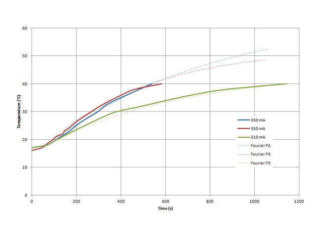
Figure 11. Module Temperature Rise
If we assume that the case heating curve will be of the form (based on Fourier’s law):
then we can use our measurements to predict the final brass case temperature of the laser at different operating currents. The final case temperature is predicted to be around 65°C at 350 mA and 45°C at 312 mA.
We can incorporate temperature compensation on the driver board with a simple temperature sensor. While we can’t directly thermally couple to the laser diode, its case or the brass housing, if we position the sensor near the laser diode leads then it should still be effective, particularly if the board is enclosed.
We need a temperature sensing component such as a semiconductor junction, thermistor, thermocouple, or proprietary IC. The 3 Volt rail voltage rules out the IC approach. I’ve decided to use an NTC thermistor because they have a relatively high -dR/dT, I have a heap in stock, and they are relatively low cost.
Two additional parallel resistors (1K NTC and 680 Ohm) with the 0.5 mA JFET constant current source provide the negative temperature feedback. The laser current is now temperature regulated at 500 mA at 10°C dropping to 300 mA at 40°C. The constant current supply is variable so we can readily increase of decrease the laser current, but noting that the temperature compensation at 40°C will be always be about 40% of the laser current at 10°C.
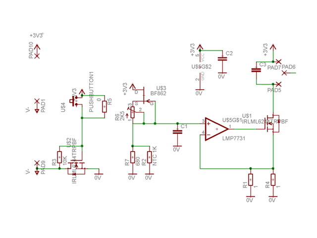
Figure 12. New Temperature Sensing Constant Current Driver
I have simulated the thermally compensated current regulation in ICAPS SPICE. Operation is good from less than 2.5 to 5.5 Volts supply. The constant current regulation works well as does the temperature negative feedback. There are no transient or oscillation modes apparent.
With component values selected I designed a new Printed Circuit Board (PCB) which measures just 11.9 mm wide x 15 mm long (cf. 12 x 20 mm) It could be made smaller with some more layout effort (perhaps 13 mm long x 10 mm wide) but I want to retain the push button 8 mm from the power supply terminal end for compatibility with my existing case, and I want lots of copper around the laser diode leads for heat dissipation.
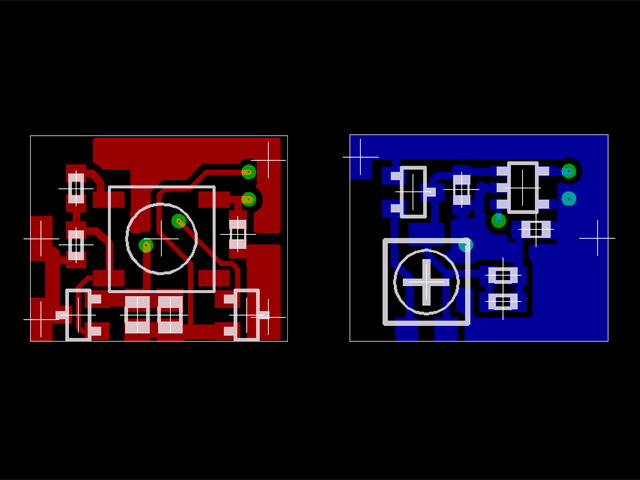
Figure 13. New Board (11.9 x 15.0 mm)
Cost
I can’t be bothered with the effort of doing a detailed cost analysis, but the new board should be lower cost that the original with improved performance. The following cost estimates are based on low quantity prices from a single industry component supplier.
The cost reductions come from reducing the switch current rating (a 50 mA tactile switch costs less than 7 cents while a 1 A push button is closer to $1), the replacement of the TL431 precision reference with a JFET and resistor (a saving of say 20 cents), and replacing the D882 NPN transistor with an appropriately rated MOSFET (a saving of 80 cents). My design adds three line items but the actual cost of these components is minimal and the total component footprint is significantly reduced.
With the reduced board area every fourth board is effectively free and I could probably improve this with a bit more design effort.
Interestingly the original LM358 op amp is literally as cheap as chips (say 10 cents each) whereas an appropriate single op amp rated with a single supply of 1.8 to 5.5 V, and with rail to rail outputs was around 38 cents. However we absolutely need the reduced Vcc range and there are savings associated with the reduced component footprint.
My replacement potentiometer is significantly more expensive than the OEM component but it is sturdy, enclosed, and has end stops. Why would anyone scrimp on a few cents at the cost and inconvenience of destroying the laser diode?
Oops, my new constant current source has two minor issues.
The JFET constant current source needs an additional resistor to limit the maximum current source current, otherwise this could be set way too high. A 220 Ohms resistor will limit the maximum laser current adjustment across all JFET parameter variations between 0.5 A to 1.75 A at 10°C. We can reduce the trim pot to a 2K preferred value so our minimum laser current adjustment across all JFET parameters is between 61 mA and 238 mA at 10°C.
The second issue is a board layout one. The trim pot needs to be adjusted so that clockwise adjustment increases the laser current (it is currently the opposite way around).
With the laser current set at 500 mA at an ambient temperature of 10°C I took the following photo of the beam projecting into a moderate height cloud base on a rainy evening. The beam will be great for pointing out celestial objects.
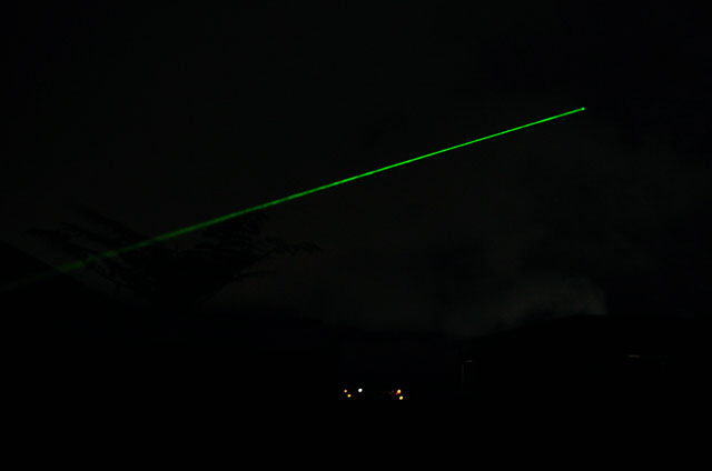
Figure 14. 500 mA Beam into Cloudy Night Sky
So now I just need to make a board, populate, and test it. This will take a few weeks as I have other stuff happening just now…
The drive board has been made, populated and tested. I haven’t bothered to cut the board to finished size as this made for easier handling during testing. While the push button switch works fine I removed it for the tests, replaced with a 0 Ohm link incorporated for this very purpose.
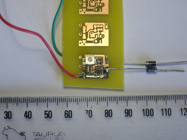
Figure 15. New Driver Board with Temperature Compensation (Bottom View)
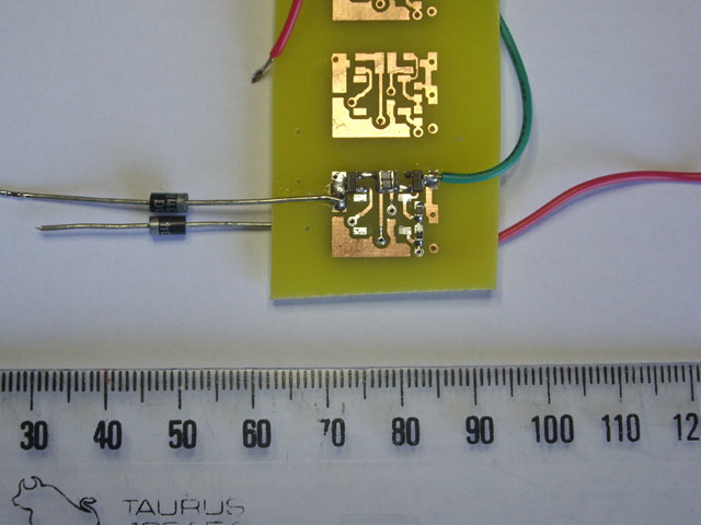
Figure 16. New Driver Board (Top View)
Push Button Removed for Bench Testing
Rather than risk the laser module I have used a couple of series connected 1N4001 silicon diodes and an ammeter to simulate the diode pump laser. At 0.5 A these have a total forward voltage drop of about 2 V which is a little above the laser at about 1.8 V, but close enough for testing.
The reverse polarity protection is working fine. The voltage drop with correct polarity is about 27 mV at 0.5 A. The reverse bias current is about 0.3 mA due to the 10K Ohm pull-down resistor.
The switching circuit works fine from a 3 Volt supply but fails from 5 Volts. The issue is the body diode in the reverse polarity protection MOSFET. The only way to overcome this is to add another MOSFET for the switching function.
The JFET constant current source works just fine with adequate adjustment. This is best set with the simulated laser disconnected because the MOSTFET source follower and the current sensing resistors cause the NTC thermistor to heat up, and the output current drops steadily.
The circuit works nicely from two AA Lithium iron disulphide batteries at 0.5 A provided that these have a reasonable state of charge.
The minimum effective voltage for 0.5 A current regulation was around 2.3 V at the board. The associated voltage drops in the laser discharge circuit are:
0.25 V across the current sensing resistor.
1.96 V across the simulated laser diode (2 series 1N4001 diodes and ammeter).
0.02 V across reverse bias protection MOSFET
0.07 V Drain Source on laser drive MOSFET
The limiting performance item is the MOSFET source follower. I could probably get another few 100 mV off the low voltage performance with a different MOSFET, but the existing component is more than adequate for the intended application.
The thermal regulation is working nicely - perhaps too well. At an ambient temperature of 18°C, 2.3 V supply, and the power on laser current set to 0.5 A, the board gets comfortably warm to the touch (but certainly not hot). The laser current drops from 0.5 A to 0.4 A in about 30 seconds, and has a steady-state current of 0.33 A.
Operating from 5 V the board gets uncomfortably warm (but not so hot that you can’t keep hold of it) and the laser current reduces from 0.5 A to 0.4 A in less than 7 seconds, and about 0.25 A in the steady state.
Maybe I need to reduce the thermal coupling between the output MOSFET and the NTC thermal sensing resistor? Note that the NTC resistor is not getting hot because of self-dissipation:
While the board performs well there are three physical issues that I need to resolve.
The board dimensions are quite small (12 mm wide x 15 mm long), but in pressing for the reduced size I have stuffed up the dimension between the tactile switch and the end of the board. So I need to make the board a bit longer.
The current adjustment potentiometer is mounted too close to the edge of the board and may interfere with the case. I need to centralize this on the board.
The tactile switch that I have used is somewhat taller than in the original laser module. This makes actually mounting the laser module in the existing case with a water proof actuating button and membrane all but impossible. I’ll need to think about how best to resolve this.
I’ve got some new SMD tactile switches on order that are just 2.5 mm tall, the PCB has been adjusted to get the switch back in the right place, the current adjustment pot is now centralized, and I have reduced the thermal coupling between stuff that gets warm and the NTC thermistor. The new board dimensions are 9.4 mm wide x 20.7 mm long.
After considerable thought, I’m going to have to remake the case front housing and window. While I can make the new module fit the existing case, fitting of the switch actuation plunger is going to be difficult, the electrical connection between the laser module and the case isn’t robustly positive, and the alignment of the switch with the plunger is tricky.
More to follow…
|