|
I need a programmer for the Amigo. The programmer needs to provide rapid secure connection to an Amigo PCB from a USB port, a regulated 3.3 V DC supply, a Go/No-Go current monitor, and an ISP interface.
During the Amigo development I have used a number of different clip arrangements for programming. While they worked, they were difficult to align and fit and were far from adequately secure.
The Go current limits are less than 1 mA but for the purpose of this description I have established arbitrary Go bounds of 10 and 20 mA. Power is provided from the 5 V rail of a USB port.
The current monitor is required to establish whether or not there is a board fault prior to programming. While I could use an ammeter the programmer is ideally a stand alone device and detailed current measurements can only be completed after programming as the software controls a number of peripheral circuit blocks that determine operating mode - some of which draw significant peak currents.
My initial design for the current monitor circuit is shown in Figure 1.
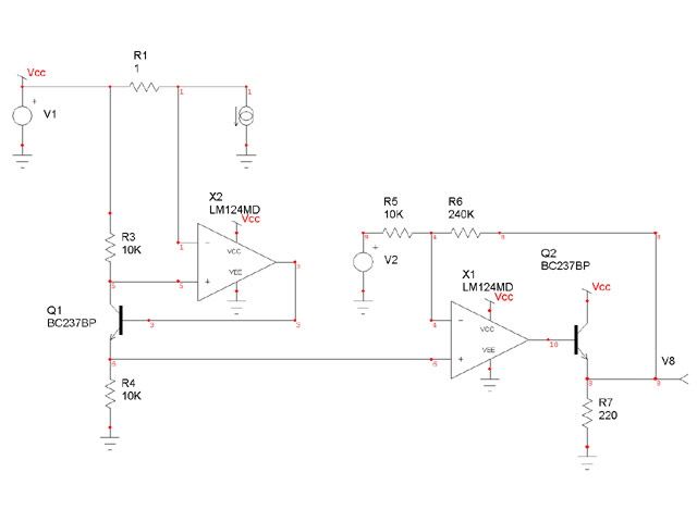
Figure 1. Initial Current Monitor Design
The Go/No-Go circuit is based on two functional blocks: a current monitor and a series of voltage comparators.
The current monitor uses an op amp to develop a voltage at the non-inverting input equal to the current sense voltage drop across R1. The voltage drop across current sensing resistor R1 is applied to the non-inverting op amp input by inverted feedback. The output voltage is measured relative to Ground across R3 as Iload * R1 / R2 * R3 / α Volts per Amp where α is a the ratio of collector to emitter current in the BJT.
This circuit works beautifully in theory. It provides some gain and it draws virtually no current from the current sensing resistor (just the bias current of the op amp inverting input). However it is difficult to implement with off-the-shelf operational amplifiers because both the inverting and non-inverting inputs are operating at or near the positive supply rail. This exceeds the common mode input voltage range for many op amps which typically extend to Vcc – 1.5 Volts. Either we need a ‘special op amp’ such as an LM7332 or we need a different design approach.
Let’s try a standard differential amplifier configuration as shown in Figure 2.
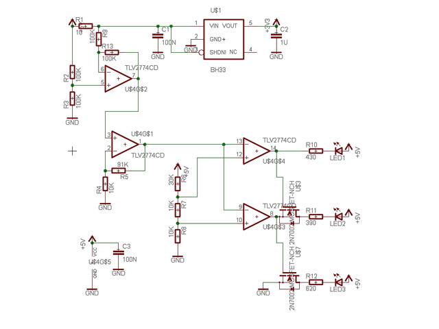
Figure 2. Differential Amplifier Current Monitor Design
(complete with 3.3 V regulator and LED drive comparator)
The circuit overcomes the common mode voltage range problem because it is operating with the op amp inputs near Vcc/2. However it provides no voltage gain of the current sense voltage developed across R1 (Vout = I load * R1). Voltage gain has to be added elsewhere and I have used a second non-inverting op amp with a gain of 10 for this purpose. The current monitor also has the disadvantage that the current through the inverting input resistor divider varies with actual load current and contributes to the measured load current. We can make this additional current component quite small (say 1000th of the anticipated maximum current of interest) by making the resistor values connected to the inverting input relatively large.
The design uses a 3.3 V LDO linear regulator rated at 150 mA with thermal shut down and current fold-back limiting. I have used a ROHM BH33 regulator in an SO23-5 package. This regulator has a very low quiescent current of around 40 uA which is desirable for this application.
The regulator is quite straight forward and requires little further explanation other than to note that the Standby pin on the BH33 must be held at > 1.5 V for operation, and an output capacitor of at least 1 uF is essential to avoid oscillation.
The output comparator design is relatively straight forward. Sense voltages are established by resistor divider R6, R7, R8. Two further op amps are used to compare the current sense voltage with the established voltage trip points and turn on LEDs.
A conventional series of stacked comparators will turn on the LEDS sequentially. This is not desirable in this application because as more LEDs turn on the load on the USB port increases. Two MOSFETs were added to provide a point type (only one LED on at any time) display.
The circuit was constructed using a relative standard LM7224 quad rail to rail output op amp and worked beautifully first time. Trip points are established at 10 mA and 20 mA and the LEDs sequence nicely. The total current of the monitoring circuit from the USB port is just 8 mA (comprising 5 mA for an LED and 3 mA for the op amps). The monitored current offset is just 65 uA comprising the regulator quiescent current and the current drawn through the current monitor inverting input resistor divider. This was compensated for by adjusting the sense voltage resistors R6, R7 and R8 with a final trip point accuracy of less than +/- 0.1%. With a 10 Ohm voltage sense resistor, R1, the 3.3 V LDO regulator will supply a 125 mA load before drop out – well within the anticipated maximum load, but somewhat less than the 150 mA current fold-back limit of the regulator.
The circuit was built of a double sided PCB measuring 31.5 mm x 23 mm (about the size of two postage stamps) and assembled in a 3D printed case.
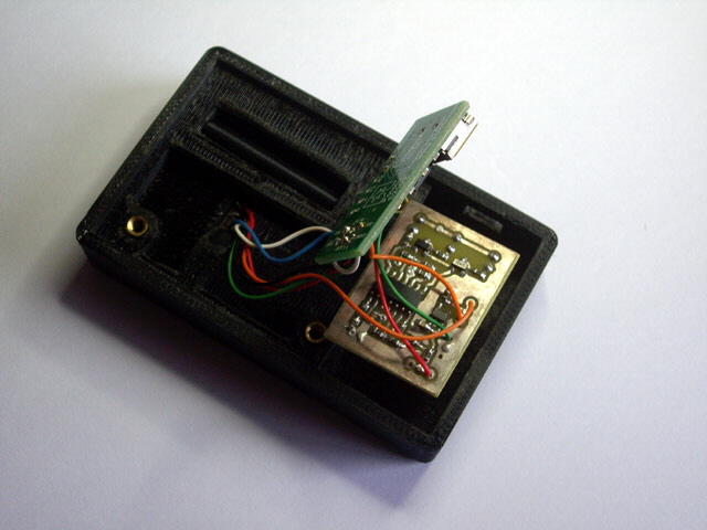
Figure 3. Current Monitor and Regulator PCB
The Amigo Boards can now be secured with absolute physical accuracy in the programmer in just a couple of seconds and fully programmed in less than a minute. Any issues with board current can be identified and resolved on the programming platform.
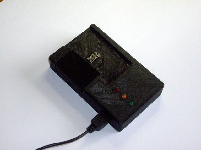
Figure 4. The Assembled USB Programmer with Current Monitor
But perhaps there is another way of doing this using conventional op amps? We are somewhat constrained by available supply voltages but the following design idea works in practise. Figure 3 shows the suggested circuit.
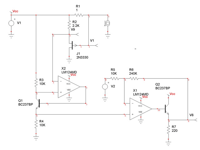
Figure 5. JFET Source Follower Current Monitor Design
We have added a P channel JFET as a source follower across the current sense resistor R1. This operates in the saturated region (pinch-off) because the source to drain voltage is > Vp. The source voltage follows the gate voltage, but with a gain of slightly less than 1 and with a DC offset determined by the JFET parameters Vp and Idss and the source resistor R2. Ideally we want to operate the JFET with a gate voltage almost Vp greater than the source to reduce output non-linearity due to the imperfect drain current source in real JFETs.
The only current through current sense resistor R1is the load current, Iload, as the JFET gate current is essentially zero. And the current measurement voltage at the JFET source is now less than Vcc – 1.5 V. We can measure this using the op amp current monitor circuit of Figure 1.
I have also added a non-inverting gain stage with a 4.6 V Zener regulated offset adjustment, and an output emitter follower to ensure that the output can track to ground. The Zener (or some other form of regulation) is necessary on the offset to reduce the effect of changes in Vcc due to load on the output.
Circuit design with discrete JFETs is complicated by the variability in the device parameters, Vp and Idss, but these are easy to measure and resistor values can be adjusted accordingly, either using ready reckoning, or by relatively straight forward (but somewhat tedious) hand calculations, or a circuit simulator. I like to use a simulator which also lets me investigate a heap of other stuff such as dependence on temperature and Vcc, but for the record here are the other two design approaches for the JFET source follower.
We need the source voltage to be at least 1.5 V below Vcc (this is the whole purpose of the circuit) and the JFET needs to be operating in the saturated region. Our signal swing is determined by the current sense resistor R1 and the maximum anticipated load current. This needs to be relatively small in order to minimise the voltage drop to the following 3.3 V regulator (0.1 V at 100 mA gives us a current sense resistor of 1 Ohm), and < Vp. We can assume that Vcc is relatively stable at 5 V under the anticipated load currents as a USB port should happily source 500 mA with a mminimum voltage of 4.75 V.
For the JFET to remain in saturation the drain voltage must be at least Vp below the source voltage. With Vcc = 5 V with Vp of 1 to 3 V should be fine with the source voltage of less than Vcc - 1.5 V . Let’s run with Vp = 3 V. Note that Vp is positive because we are working with a P channel JFET.
We can estimate our source resistance, R2, as (Vcc – the desired source voltage) divided by the assumed 1 mA drain current: = (5 – 3) / 1 mA = 2,000 Ohms.
We can also calculate the source resistor somewhat more explicitly. In saturation the relationship between Vgs and Id is described by the following (simplified) equation:
Vgs is the gate to source voltage and it will be set by the JFET characteristics and both the current sense resistor, R1, and the source resistor R2. We want the JFET operating in pinch off but with enough headroom to avoid being cut off under maximum current load. We want the sense current to be relatively small compared to the load current , say 1 mA, for efficiency.
We already know that a source follower has a gain of slightly less than 1. Voltage gain will be provided elsewhere in the current monitor circuit.
In order to determine the source resistance R2 we can replace Vgs in [1] with:
Vgs = Id * R2 – Iload * R1
Id = Idss (1 – (Id * R2 – Iload * R1) / Vp)2 [2]
This is a quadratic where everything is known except R2. We just need to solve it (this is the tedious and error prone bit).
Expand out [2]:
Id / Idss = 1 – 2 * (Id * R2 – Iload * R1) / Vp + (Id * R2 – Iload * R1)2 / Vp2
Id / Idss = 1 – 2 * Id * R2 / Vp + 2 * Iload * R1 / Vp +
Id2 * R22 / Vp2 – 2 * Id * R2 * Iload * R1 / Vp2 +
lload2 * R12 / Vp2 [3]
Now we get [3] into Standard form ax2 + bx + c = 0 (also called collecting terms) where x is the unknown resistance, R2:
a = Id2 / Vp2
b = - 2 * Id / Vp – 2 * Id * Iload * R1 / Vp2
c = 1 + 2 * Iload * R1 / Vp + Iload2 * R12 / Vp2 - Id / Idss
Note that the units of each of the terms a, b and c are consistent and we have the same number of terms as [3] (both useful sanity checks)
Now we can plug in our known values and solve for R2 using the familiar:
where: Id = 0.001 A
Vp = 3 V (say)
Iload = 0.1 A
R1 = 1 Ohm
Idss = 0.013 A (say)
So:
R2 = 2,267 Ohms or 3,932 Ohms.
Only one of these solutions is valid. Clearly if Id is 1 mA and R2 is 3.9 K Ohms the JFET will be cut off so R2 must be ~ 2.2 K Ohms. This is reasonably close to our rough and ready estimate of 2 K Ohms.
We can expect that the source voltage will be about 3.1 V, dropping to about 3 V under full 100 mA load.
We can also use [2] to calculate the actual voltage gain of the source follower. The drain current, Id, changes from 1 mA under full load to:
We need to solve this quadratic for Id0. The solution is Id0 = 0.648 mA. The source follower voltage gain can be calculated as:
This determines the gain required in out buffer amplifier. Lets say we want 2 V output for full load current of 100 mA.
Actually building the circuit requires hand selection of a JFET with a Vgsoff of about 3 V. This isn’t difficult but you will need a bunch of JFETs to find one with an appropriate value. While I haven’t studied the distribution of the parameters Idss and Vgs, they tend to track together and are probably Normally distributed for a given batch between data sheet limits.
Job done, but please email me If you have any suggestions or questions about this design.
|