|
At 20 Feb 17 I have a reliable 600 Watt Second welder that will deliver about 10,000 Amps. The welder is robust - it will survive static discharge and all manner of abuse including a discharge with coiled welder cables around a metal core into a dead short. Many commercial welders won’t survive this torture test (indeed they specifically advise against coiling the weld cables). This isn’t a toy - do read the warnings.
I have need of a Capacitive Discharge (CD) welder in order to progress the Amigo commercialization, for making thermocouple beads, and for a number of other applications including appliance servicing. A commercial unit will cost about $NZ 5,000 - which means I have about a four weeks to develop and make a useable device.
Warnings
- This welder is capable of generating significant magnetic fields during the discharge pulse. If you have a pacemaker or other medical implant then maybe you don’t want to be making or using a CD welder.
- CD welding produces intense localized heating , arc flash and weld spatter that can cause eye damage, cause burns, and start fires. Wear appropriate safety equipment and take appropriate fire precautions as for arc welding.
- Wristwatches and other instruments can be damaged by strong magnetic fields. (I have already damaged my Seiko wristwatch using my welder. The repair was very expensive.)
- Any constructor should ensure sound wiring techniques and fuse protection for mains operated equipment in accordance with jurisdictional regulations and prudent safety
requirements.
- This design documentation is work in progress. Please read all of the associated pages to ensure that you don’t repeat my errors before starting construction.
The basic principle of CD welding is to pass a large current (perhaps several thousand Amps) through the weld junction resistance in a very short time (a few milliseconds). The heat generated by the delivered power in the weld junction does not have sufficient time to dissipate and melts the adjoining metals forming the weld.
Dual pulse welding uses an initial pulse to heat the weld junction, vaporizing surface contaminates immediately prior to a secondary current pulse that forms the weld. This improves the integrity of the finished weld and is therefore desirable.
There are a number of internet sites that provide information and schematic diagrams of pulse welders including:
Having examined the commercial and home made offerings I have decided to make my own building on earlier designs. While these earlier designs clearly work there are a number of opportunities for design improvements that I intend to implement.
- The MOSFET switch that controls the current discharge across the weld junction needs to switch fast (nano seconds) to avoid wasting power and heating of the MOSFETs. Referenced designs turn on relatively fast but are slow to turn off. Optimal switching requires that the MOSFET gate capacitance is actively charged and discharged.
- For optimum component heat dissipation, power components should be directly connected to heat sinks without intervening FRP circuit board or other electrical insulation. Further, the heat sinks should present a vertical convective profile, unless subject to duct-directed fan forced cooling.
- Circuit reactance (resistance and impedance) in the discharge path should be minimized. Wide, short conductors should be used and these should have significant surface area to account for skin effect. Current tends to flow in the outer surface of conductors at high frequencies (and during transients).
- A number of published designs use potentiometers for establishing operating parameters such as discharge time and voltage. Potentiometers are inherently noisy and potentially subject to EMI in close proximity to high current discharges. I’ll be attempting to use Grey code rotary encoders. These will also allow me to set operating parameters in the software at any time, independent of the rotary position and provide precise digital control of the resolution of associated parameters.
- The capacitor charge and discharge circuits should be current-limited to match the rating of the power supply during turn on and during changes in capacitor voltage.
I’m using ten 200 A MOSFETs in the main discharge path with a pulse rating of almost 10,000 A. Because these devices should be either fully off, or fully on for just a few milliseconds with a maximum on resistance of 0.003 Ohms their power dissipation should be minimal. However the bond wire current limit requires that the devices should be kept cool. They need a decent heat sink because they will be operating near their transient thermal limits (but within their Safe Operating Area).
Construction started with the development of copper buses for the weld discharge path using a bunch of IRFP3206 MOSFETs that I had lying around. Initially I had hoped to solder or braze the MOSFETs directly to the 25 mm x 3 mm section copper bus but I couldn’t get the copper hot enough to melt the solder without using a butane torch with significant risk of overheating the MOSFETs. I need a CD welder to make direct bus welds and I obviously haven’t got one yet. I settled on a robust clamping arrangement which requires no heating process and has the the added advantage that I can replace individual MOSFETs relatively easily when I blow them up!

Figure 1. Discharge Capacitors and the MOSFET Bus
This took a day to design and a day and a half to construct, mainly because there were so many holes to drill and tap. I only had one calamity when I broke a bottoming tap in a heat sink. It took some effort to remove it. The damaged section of the heat sink was replaced with a force-fit aluminium plug which should retain thermal integrity. The repair is visually almost indistinguishable from the original.
Next mission is the MOSFET gate drive circuit. This is the most important aspect of the welder (after the bus structure) because it dictates minimum pulse width and has a significant effect on power dissipation in the primary paralleled drive MOSFETs. The starting point is Franz’s drive circuit shown in Figure 2. Note that Q3, Q4 and associated resistors are actually an integrated circuit (type UNA2003 or equivalent) modelled as discrete components.
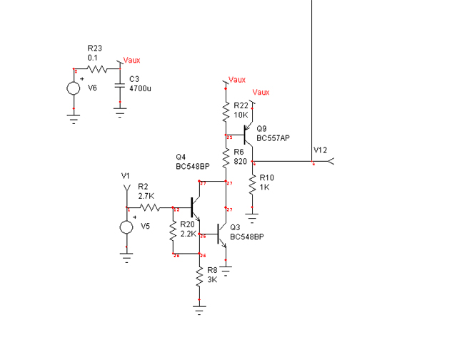
Figure 2. Franz’s Circuit (note Darling drive is ULN2003A)
This will charge the paralleled discharge MOSFET gate capacitance (around 860 nF) to about 10 V in under 1 us but the discharge characteristic is not so good, requiring about 0.25 ms for turn off. This results in relatively high power losses with short discharge pulses and limits the minimum pulse width.
I have contemplated several design strategies but settled on a discrete component 12 V Schottky TTL inverter stage with an active collector load and complementary emitter follower output stage. For testing I threw together a few regular TTL IC’s to generate the right pulse sequences while ensuring absolutely no MOSFET crossover conduction. In the welder these control pulses will be generated directly from the microcontroller (running at about 125 ns per instruction).
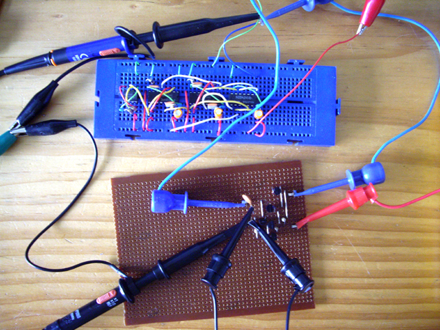
Figure 3. On the Test Bench
The circuit simulates switching the MOSFET gate capacitance between 2 and 10 V in less that 20 nanoseconds. The bench test test switched at about 40 ns limited by the speed of the logic drive (more circuit gain required for pulse acceleration). Average current draw from the 12 V rail was ~25 mA - no heat sink required. For optimal switching this needs to be mounted as close as possible to the main gate bus. I think I’ll bolt the board directly to it.
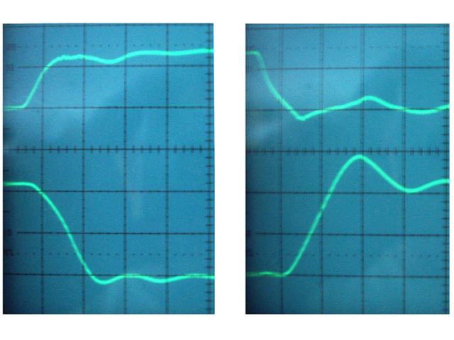
Figure 4. Switching Fast. Horz. 50 ns/Div.
Top Trace: Digital Drive, Vert. 2 V/Div. Bottom Trace: MOSFET Drive, 5 V/Div.
The drive operates substantially faster than the MOSFET delay, rise and fall times (around 130 ns) but the down side is that uses a few more components than Franz’s design. Here is one half of the circuit (Figure 5). Note that diode D2 is not required except for the purposes of circuit simulation. The other circuit is essentially identical except that the output MOSFET is a P Channel device (F9540N) with the source connected to the 12V auxiliary supply and the drain connected to the paralleled gates of the main driver MOSFETs.

Figure 5. Fast MOSFET Gate Drive Circuit
Here is the briefest description of circuit functionality. V5 is the input at TTL or 5V CMOS levels. Q2 is a common base stage when V5 is low or else a diode source through the forward biased base collector junction to the base of Q1. D1 (a Schottky diode) prevents Q1 from going into saturation which will slow its switching speed. Q4 and associated components are a constant current active drive for the input stage. This ensures that transitions are linear rather that negative exponential (a typical RC charge response) and therefore faster. The current gain of the complementary emitter follower comprising Q3 and Q4 ensures that the gate capacitance of MOSFET X1 charges and discharges rapidly.
Silly me! I have found a tube of high speed inverting MOS drivers (DS0026) which do away with my drive circuit at Figure 5 entirely. Although these particular ICs are now obsolete there are equivalent device offerings from other manufacturers.
The next design challenge (they are getting fewer and easier) is the capacitor charge and discharge circuits, simulated concept shown in Figure 6. These don’t need to switch fast but they do need to limit the current to less than 12.6A to prevent overloading my power supply transformer. As a consequence some of the components will get hot during the charge and discharge cycle so hefty heat sinks will be required - probably with forced air cooling. I plan to fit a temperature sensor to the charge heat sink. Charge and discharge characteristics are linear at about +/- 3.2 V/s between 0 and 20 V, so it should take slightly over 6 s to charge from 0 to 20 V.
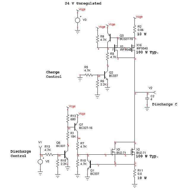
Figure 6. Constant Current Charge/Discharge Circuits
(Note: Component values updated on 24 Nov 11)
The circuit description is quite straight forward. Q2 and Q6 are saturated common emitter stages providing a standard one TTL load. Q7 is an inverting stage in the discharge control. Q1 and Q3 and associated resistors R4, R11 and R2, R9 are the current limiting stages. When the current through the parallel resistors reaches about 0.7 V the transistors start to conduct reducing the associated MOSFET GS voltage. Silicon BJTs have a negative band gap temperature coefficient so that as the transistors get hotter (through proximity to the MOSFETS) they conduct more current decreasing the associated MOSFET GS voltage. Unlike BJT’s, MOSFETs can be connected in parallel without careful matching because they tend to current share.
Throughout this design I am mindful that power levels are significant and a design stuff-up will likely result in semiconductors failing en-mass to protect the fuses. From experience such failures are instant, expensive and time-consuming. I don’t want to get into this space! On fusing, I have allowed for active MCU controlled temperature sensing of the charge and pulse-discharge heat sinks, and a passive 141°C 10 A thermal fuse in series with a conventional 2 A slow-blow fuse on the AC supply.
Thoughts. A few years back I designed and built an isolated 24 volt 20 A switch mode power supply using parts salvaged from a stuffed computer PSU and a Smart Drive washing machine. The device functioned perfectly except for the the presence of very brief voltage transients on H Bridge switching. While these were significantly less than the transients measured on the original computer supply and on comparable commercial switch mode power supplies I was not satisfied with the design. The prototype resides in one of my scrap boxes (Figure 7). The power supply for my welder is based on a 225 VA toroidal transformer that weighs more than 2 kg but limits the secondary current to just 12.6 A at 18 V RMS. For discharge cutting applications I may need to revisit my switch mode power supply design. This is not a project for Joe Average. Circuits involving direct rectified mains voltages with these current-delivery capabilities are potentially fatal.
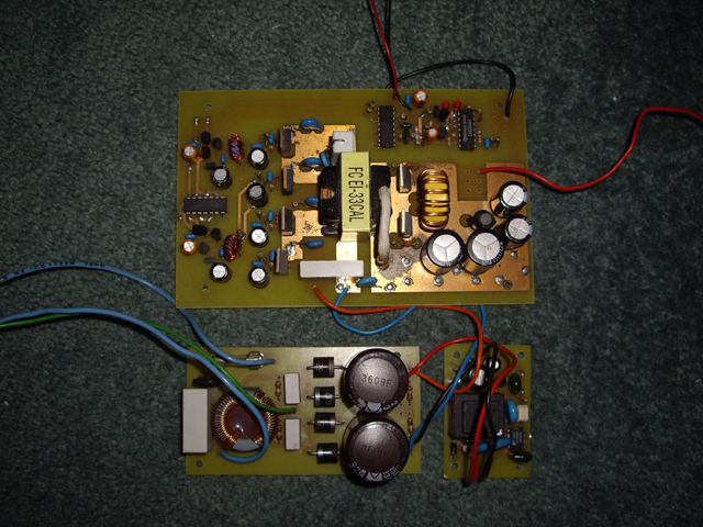
2 November and I’ve completed the design of three of the four circuit boards and the fourth is progressing well. My initial approach was to use Veroboard for construction but this won’t work for the SMD processor board or the high currents associated with the main capacitor charge/discharge circuits. I’ve settled on four boards because this allows each board to be mounted close to the discrete heat sink mounted power components it controls. The modular design also allows ready replacement of any section of the circuit and aids with construction and testing.
3 November and the board designs are finished at last. There have been a few minor design modifications in the process, mainly to ensure fast compatible drives between the digital and analogue stages. The processor board has been the biggest challenge and it is covered with DIL connectors for:
- LCD drive.
- LCD backlight supply.
- Four Grey Code rotary encoders for capacitor voltage adjustment, inter-pulse dwell and dual pulse times (interrupt driven).
- Pulse trigger input (interrupt driven).
- SPI programming interface.
- Six high speed TTL buffered drivers for charge, discharge, pulse on, pulse off and two auxiliary.
- Capacitor voltage monitoring with over-voltage and current protection.
- Two temperature monitoring interfaces.
- Power connection to the on-board regulator.
- Four auxiliary MOS I/O ports for LEDs, buzzers and all of the stuff that I have failed to anticipate a need for.
4 November and I didn’t quite get to make the PCBs today as planned although the artwork is printed. Because of all the IO requirements I’ve gone for an Atmel ATMEGA128 processor with 64 SMD pins to route. It features a heap of external hardware interrupts which makes interfacing the rotary encoders a breeze. As usual I like to write my code with a simple flow chart, breaking each functional block into successively smaller blocks of less than about 20 lines of code. Figure 8 shows the top level flow chart. There is one main routine, five interrupt entry routines, and two background watchdog and power brown-out routines (not shown). As there is only one timing-critical routine the code could be readily implemented in C although I will probably stick to Assembler for optimized code length and precision discharge pulse width.
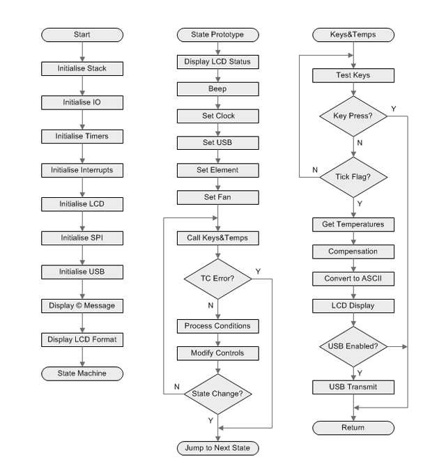
Figure 8. Top Level Flow Chart
5 November. Three of the boards are etched and drilled but they are all going to get a thick tin plating to increase the conductor thickness (every micron helps). I should have got all the boards made today but my trusty Dremel stopped working with a horrible ‘something is definitely broken’ sound. One of the rotor brush contacts on the commutator had come adrift and the resulting sharp edge had pulled one of the brushes into the gap between the stator and the rotor. The long and short of this was a trip out to purchase a new Dremel.
The pulse control circuit has been built and tested. The circuit diagram and board are shown in Figure 9. When switching this fast you can expect transients with reactive loads so the snubber is essential to avoid ringing. Circuit performance into an 0.1 uF load with lead inductance is shown in Figure 10 switching from 2 V up to 10 V in 55 ns and from 10 V down to 2 V in 40 ns. The propagation delay is about 50 ns. All good!
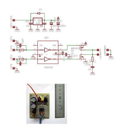
Figure 9. Pulse Control Board (how simple is this!)
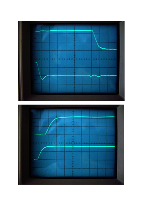
Figure 10. Pulse Control Board Performance. Horz. 50 ns/Div.
Top Traces: Main MOSFET Drive, Vert. 5 V/Div. Bottom Traces: TTL Drive (high side), 2 V/Div.
9 November and I have remade and tested the charge and discharge boards after identifying an earlier design fault. The testing was limited to 1 A from 12 V because the MOSFETs were not mounted on their heat sinks and they get uncomfortably warm in a few seconds dissipating 12 W, power limited due to my bench power supply (a home made +/-5 V +/-12V supply with a 1 A current limit on the 12V rails). The MOSFETs switch on fast but turn off takes about 500 ns. However this is not critical because the main discharge capacitors should limit the voltage rise to a few uV in this time and the MOSFETs are already dissipating around 100 W each (but for no more than 7 s). The amended circuit is at Figure 6 and a photo of the two boards in position but not yet mounted on the heat sinks is at Figure 11.
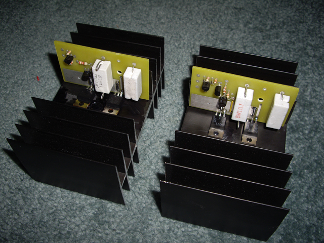
Figure 11. Charge and Discharge Boards Good to Go
This project has already taken two weeks and I have much to do :
- mounting the boards to their respective heat sinks and the main discharge MOSFET gate bus (say 6 hours)
- writing the software to implement the flow chart at Figure 7 (three days).
- making, populating, programming and testing the MCU board and connecting to the LCD and rotary controls (the artwork is done but this will take at least three days).
- wiring the main 24 V unregulated power supply and heat sink mounting (6 hours).
- fitting the heat sink stand-offs (already machined) and bolting these to something more substantial than my office carpet (6 hours)
- ordering some rotary encoders and a few more 5 W resistors for current tuning (delivery in 8 days and fitting in 3 hours).
- machining the discharge electrodes, fitting a discharge control and the high current wiring (one day).
The critical path through all this is at least 10 days and with slippage I expect it will take two weeks to complete the design to a bare-bones, uncased working unit. Best I add a few days for testing, so I figure I have about three weeks to go. Maybe purchasing a commercial unit wasn’t such a bad idea after all?
I have been thinking about making up a kit set based on my design with all of the hardware and components, but without a case. if anyone is interested then please contact me. The only really tricky bit is the MCU board and this will come pre-assembled and pre-programmed due to the SMD processor, but complete with an SPI interface and source code for those ambitious enough to play with the code and risk destroying their welder. I have no idea of the likely cost just now (other than it will be less than half the price of a commercial device). I figure that the kit could reasonably be assembled in two full days. Yes, I’m prepared to support constructors that run into problems but while my time is not expensive, it is not free.
10 November and the few bits that I haven’t got are on order, the MCU board has been made (but not populated) and I’ve designed the discharge electrodes. This evening (once I’ve completed web site updates) I’ll be making a start on the MCU code.
11 November and the MCU board is finished. Although I haven’t tested it yet other than for continuity across vias and a visual inspection of the soldering but I don’t expect too many problems. This is essentially a standard Atmel ATmega128 running at 8 MHz with a 5 volt regulated supply and all of those input and output connectors that I have already talked about.
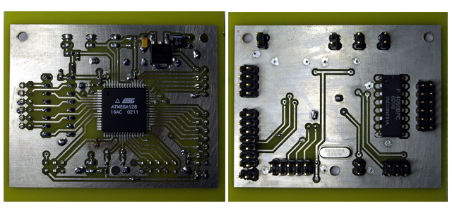
Figure 12. The MCU Board Assembled
(schematic to follow after software development and testing)
The code is progressing well. The top level structure has been written - but I have yet to delve into the application-specific subroutines. I’ll be starting with the LCD interface - simply a matter of porting some code from an earlier application across to this project and modifying it to suit the allocated ports and an 8 bit bus structure. In the past I have used the LCD’s 4 bit data bus to conserve I/O but in this application I have gone for the full 8 bit bus.
12 November and 80% of the application specific code is complete including the timing-critical weld pulse routines, the LCD drive and the rotary encoder interrupts (which include essential switching de-bounce). I figure that the last 80% of the code (no - not a typo) will take another day to complete followed by testing to ensure that when I blow something up I do it properly. The only other progress for today has been mounting the main 24V unregulated supply bridge rectifier on its associated heat sink and applying power to the processor board. Vcc is right where it should be, and nothing is getting hot! Tomorrow I hope to finish the code and begin testing, starting with the LCD interface, then the critical pulse drive, followed by the charge and discharge routines.
13 November and after an early start the code is almost ready for testing and it’s only just gone 9 am. While writing the code I have come up with a few hardware improvements for later versions including incorporating a piezoelectric sounder and the mains detection circuitry directly on the MCU board and increasing the size of my 16 x 2 character LCD display module. I have also added a few common sense warnings at the top of this page. Please read them.
It is now the end of the day and the code (written in under two days from scratch in less than 1,400 bytes of Assembler) compiles and simulates without error. Sorry dudes, but I have no cool pictures or graphics to post from this concerted effort. There is nothing particularly special about the program and I have put no effort into optimizing it. There are a number of routines that can be sped up and code-optimized starting with the hexadecimal to ASCII display routines that currently uses a subtract and compare algorithm, that would be much faster and smaller as a sequence of look-up tables. However I have put some effort into ensuring that the rotary encoders, power down signal and weld trigger pulse switches are fully software de-bounced, and full discharge of the pulse capacitors and the main supply capacitor on power down (without bleed resistors which waste power under normal operation).
On this last power-down discharge issue the hardware and software work as follows.
The main software control loop senses AC failure or power off at at time when the main 24 V unregulated DC supply capacitor (47,000 uF at 24 V) and the auxiliary 12 V regulated supply capacitor are fully charged. The power down routine disables any further actions, discharges the 4F discharge capacitors using the remaining charge in the auxiliary 12 V supply. Then, if the AC power is still disconnected, the remaining main supply capacitor charge is dumped into the discharge capacitors forcing the MCU to switch off within about 5 ms and ensuring that nothing is left energized above about 0.5V. Leakage will take care of the residual charge.
My mission tomorrow is to upload the code to the MCU board (a simultaneous test of the SPI programming interface) and start checking out the board IO using dummy inputs. My rotary encoders are still on order so the control interface test is on hold for now.
15 November and the software is up and running (so clearly the SPI programming interface is also working). There were a few problems with my initial code, mainly due to adjusting my mindset from the processor used in the Buddy Locator to the ATMega 128 (a processor which I haven’t used in eight years).
The majority of the LCD screens in typical operating order are shown on the right (excluding the over-temperature display which I forgot to photograph). As noted above, my LCD display is too small to show everything that I would like, so on power up there is a prompt that displays for a few seconds to remind you of what each number represents. The bottom right hand of the display contains the STATus message. All of the modes are supported with audio signals from a 1 kHz piezoelectric sounder.
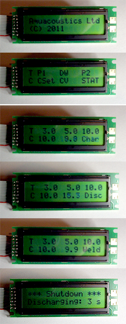
Figure 13. LCD Display Sequence
I have set the initial operating parameters as shown in the the third, fourth and fifth images in the Figure, where time is in milliseconds and voltage is in volts complete with leading zero suppression. I will need to adjust these after I make some welds and find out what works. Alternatively I might commit these to EEPROM so the welder powers up with the last settings - Yeah, I like this idea but it will require a few more hours of programming and testing.
Every mode incorporates appropriate interlocks to prevent silly operations - like trying to simultaneously charge and discharge the main main capacitor bank, or trying to weld when the capacitor voltage is not within 0.05 V of the set voltage
There was only one required minor adjustment to the MCU hardware (associated with the weld trigger input). This has been incorporated in the PCB design.
One minor hassle in the MCU Board testing has been with all of those connectors. I thought I had a whole range of double-row 0.1” rectangular headers with crimp inserts in stock but actually these turned out to be single row devices. I have ordered a range of double row headers today and improvised for testing. A word of advice if I may be so bold. If you are using crimp connectors then you absolutely need to get the specified crimping tool. Unless you intend to solder every crimp connection nothing less will do. You don’t want, or need, to find this out for yourself.
There are a few additional hardware measurements that I need to complete to ensure that the drives to the ancillary boards are appropriately sequenced and timed. While I’ve simulated the presence of the rotary Grey code encoders I can’t actually test these until they arrive from the supplier (hopefully later this week). However there is much I can be getting on with - starting with wiring up the primary power supply.
Today (actually yesterday - but it is later than I thought) was spent completing the hardware measurements on the MCU board, tidying up the code and incorporating a few software improvements including saving the last settings to EEPROM on power down, and incorporating look up tables for the temperature sensors and hexadecimal to ASCII conversions to improve processing speed and optimize resolution. The hardware tests show that everything is sequencing and timed perfectly. There are no apparent faults after many power cycles. I’m confident that the MCU board and associated code are done - subject to the performance of the rotary encoders. The supply current is just 24 mA including the LCD and on-board regulator quiescent draw.
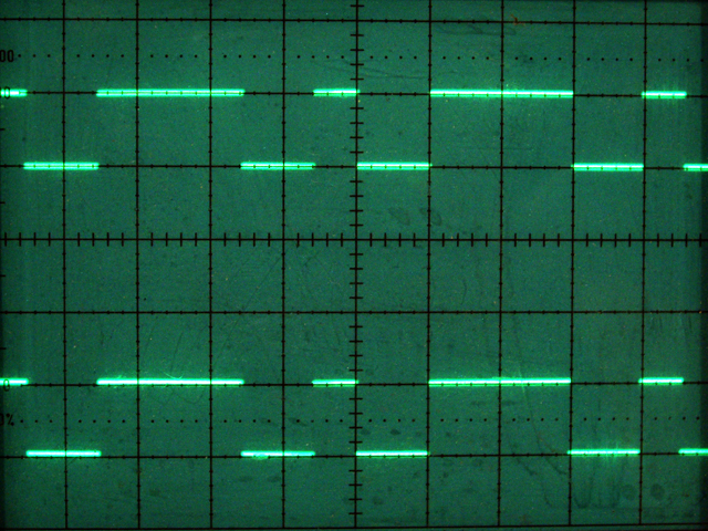
Figure 14. MOSFET Gate Control Firing Sequence. Horz. 5 ms/Div. Vert. 5 V/Div
Pulse 1: 3 ms, Dwell: 5 ms, Pulse 2: 10 ms (Defaults)
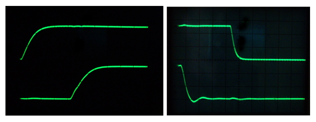
Figure 15. Gate Control Timing. Horz. 100 ns/Div, Vert. 2 V/Div.
300 ns delay to prevent MOSFET cross-over
The last design challenge has been the power sense circuit shown in Figure 16. It is a current limited full wave rectifier driving a Zener regulator with an 0.02 s time constant RC load. It connects across the secondary of the main power transformer in parallel with the power bridge rectifier.

Figure 16. Main 24 V Supply and Mains Power Sense Circuit
Time to start wiring up the main power supply, complete fitting the heat sink mounting brackets and then connecting the boards together. I was making good progress this evening with the power until I ran out of insulated crimp spade connectors. This is really annoying because I have a plastic bag full of these somewhere but I simply cannot find it. Phasing of the transformer’s secondary windings is complete and I have added a 5 A EMI filter module to the primary of the supply mainly to stop transients being injected back into the mains.
18 November and the main power supply is wired up and working, providing 26 V unregulated DC under no load (Figure 16) although it is still unsecured, just sitting on the carpet. There is a Regulation non-compliance in this image. Can you see it? It has been corrected. The problem is detailed in the next paragraph. From the photo you will see that I have extended the connections to the transformer primary with soldered double-back strain relief connections insulated by red heat shrink. The reason for these is that crimp connections on the primaries kept failing under moderate stress. I have also made allowances for the chassis-mount mains connector and fuse holder so I don’t have to remake the circuit when it eventually gets installed in a case. Much of the day was spent measuring and drilling all the holes for the heat sink brackets to allow for floor or wall mounting while maintaining a vertical airflow profile, making crimp connections, and thinking about the final case layout (Figure 18). The overall case dimensions will be approximately 300 mm wide by 350 mm long x 200 mm high with room for a decent fan. Although there are only seven components on the power sense board (Figure 16) I have decided to make another PCB for this that will mount on the main rectifier heat sink to ease kit set assembly. I am also contemplating a redesign using opto-isolators. I may also need to make a further PCB for mounting the rotary encoders so I will hold off on making the boards until the encoders arrive. For now I plan on simply bolting everything on to a piece of MDF.
And the non-compliance? The chassis earth lead is shorter than the neutral connection and the second phase connection. Should connectors physically fail under stress the last one to be placed under tension should be the chassis ground. This way the appliance shell should remain grounded until all other connections have failed.
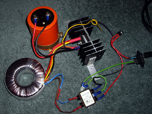
Figure 17. Main Power Supply
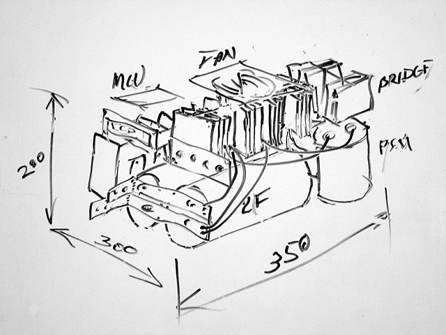
Figure 18. Case Layout Concept
19 November and the charge and discharge boards are mounted on their respective heat sinks, and I started cutting up bits of MDF to bolt everything to. All was progressing well when I remembered that I had some old steel desk top computers that had been rescued from a garbage skip (yeah - I am a dumpster-diver from way back). With just a slight modification of my Figure 18 concept, a few extra cut-outs, and some sheet bending everything fits well into a recycled computer chassis with lots of clearance around stuff that is expected to get hot. The only problem is that my electrode connection tabs are too short to use the second hole because I hadn’t allowed enough clearance for the main capacitor terminal bolts (yes - a design fault). I will have to remake the connections using the existing buses as drilling guides.
The layout works well in terms of keeping signal and power connections short, mains away from extra low voltage, and all of the heat sinks vertical. All of the wiring is appropriated sized for anticipated current carrying capacity and the wires are shown approximately routed in Figure 19. Because the weld discharge path is entirely through the copper bus structure my design does not require large cross sectional area cables. The overall chassis dimensions are 385 mm wide x 395 mm long x 150 mm deep (only 8% less efficient in terms of volume than the concept) and it weighs just on 10.5 kg.
Tomorrow will be another busy day - remaking the electrode buses, marking out and drilling a heap of mounting holes, fitting a fan (powered by the auxiliary 12 V supply that will be completely useless until the case is fitted), and continuing to progressively connect stuff together. The main MOSFET gate drive connections will use 1.5 mm wide solder braid insulated with heat shrink. This will work well with my existing bus clamp structure and provide a low inductance path from the board to the bus (a distance of about 70 mm).
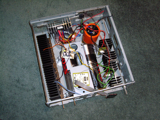
Figure 19. Fit-Out using a Recycled PC Chassis
It is timely to reflect on how this project is progressing against the anticipated timeline and budget. I still have one week to go to make a working device to meet my immediate needs and if my rotary encoders and current sense resistors arrive in the next couple of days then I expect that the project will be finished within the anticipated timeline. A significant amount of this time has been in original design development of the associated hardware and software as opposed to simply copying someone else’s design. I figure that if I had my design today and the associated components I could build this CD welder in lest than three days.
On actual cost this project has come in at approximately $NZ 1,000 to date, excluding material that have been salvaged or was in stock such as the chassis, charge, discharge and rectifier heat sinks, the secondary bridge rectifier, the main MOSFETs, wiring, nuts and bolts, etc. The main costs have been the transformer, discharge capacitors, heat sinks, copper buses, the auxiliary MOSFETs and PCBs. This is a one-off project and costs could be reduced significantly with bulk purchases.
While I am happy to publish my design efforts and software unconditionally in the hope that you can use, or build on, my efforts (as I have built on the efforts of others) I would appreciate some feedback, critical or complementary. I will reply to your email. Please take a moment to contact me and let me know how I can make Turtlesarehere.com even better for you.
Today was spent rebuilding the buses to increase the length of the weld lead attachments, removing burrs, cleaning the copper, remounting all the MOSFETs with thermal paste and marking out holes in the case. Figure 20 shows the gate and source connections for the main MOSFET drive using 1.5 mm solder wick in the centre of the bus. These connections will be insulated with heat shrink. They are really robust - the braid will fail before it pulls loose. You can see how the copper clad FRP insulator has distorted around these connections, and the MOSFET drain and source leads. This indicates a really positive mechanical bond. Note that the machine screws are electrically connected to the drain but are fully insulated from other terminals by a plastic sleeve (within the bus) and an insulating nylon washer. The M3 metal washers are there to ensure that the nylon washers do not distort under the load. Each machine screw was tightened an eighth of a turn from initial resistance in sequence until until they would not move by hand using a screwdriver with a 20 mm diameter handle. If I make a kit I will give torque settings for these fasteners to ensure positive physical connections without risk of thread failure.
(Revised 15 Feb 12) I expect that the the drain and source bus electrical connections will improve during the first few welds despite the current induced force pushing the bus apart. Through MOSFET current sharing those connections with higher resistance (P= I R^2) should get hotter and can be expected to weld to the buses. In effect the connections should be self-healing.

Figure 20. Gate Drive bus Connections using Solder-Wick Braid
The case mounting has been finally sorted but I still have about 60 holes to drill (30 for ventilation below the heat sinks) and I need to mount the temperature sensors. These tasks will have to wait until tomorrow. I’ve had a few thoughts about the front and rear panels and, if necessary, the design of a plenum that will mount under the lid that will direct fan forced air flow over the heat sinks.
21 November and everything is mounted securely in the chassis and all of the power wiring is completed very similar to Figure 19. With this prototype there were a few bolted connections that were difficult to make and I will need to rethink these for a kit set. I have earthed the positive electrode of the main discharge capacitor. This means that the negative and positive rails will move relative to earth as the main discharge capacitor set voltage is adjusted - but no current should flow in the in the ground circuit. Further, the discharge electrodes are now absolutely grounded, even during the weld pulse, so there should be no issues with welding of grounded objects, or inadvertent electrode connections to the case. I have removed the associated warning.
Rather than risk destroying my two 2 Farad main discharge capacitors (these were relatively expensive) through inadvertent over-voltage I have connected a temporary 0.047 uF 100 V capacitor across the discharge bus and written some code to test the charge and discharge routines at about 1 A. This test will be completed tomorrow.
22 November and the CD welder is now charging and discharging under microprocessor control, holding weld voltage to within 0.05V of the set point, and making appropriate beep noises and status indications on the LCD. Although nothing gets hot at this stage (or even warm even after and extended period of charging and discharging) the over-temperature alarms are all working complete with temperature display. There were one or two issues in the day. The processor has a filter capacitor on the ADC reference line and it takes an inordinate amount of time to discharge when changing references from AVCC to the internal 2.56 V reference. I also had to find and repair a broken wire in one of the numerous ribbon cables.
Still no rotary encoders or my power resistors, but there is more for me to be working on. Tomorrow I will be wiring up the discharge board, making a start on the power sense board and thinking about the best approach for a trigger (probably either a foot switch or a button on one of the electrodes).
23 November and I have made, installed and tested the power sense board which mounts on the main rectifier heat-sink as shown in Figure 21. The change in priority (over mounting the discharge board) was the result of an inadvertent residual-charge capacitor discharge when a flying test lead came into contact with the earthed chassis. If I were to ‘accentuate the positive’ then I have made by first test weld and the welder isn’t even finished yet!
However the reality is that I destroyed three semiconductors on the discharge board because I failed to ensured that the two capacitors were fully discharged before making adjustments to the circuit. I have ‘stories from the legendary past’ about tools dropped on high voltage capacitor banks, aluminium ladders forming a connection between earth and a charged bus (this resulted in a fatality), the hazards of wedding rings and metal threads in neck ties that I should have learned from.
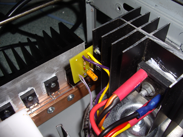
Figure 21. Power Sense Board
The power sense circuit works well. Power off is sensed within one mains cycle (at 50 or 60 Hz), all activity is halted, the main discharge capacitor is discharged at a constant current of about 10 A for seven seconds, then the power supply capacitor is discharged to the main discharge capacitor. This sequence is repeated until the processor power supply eventually fails at around 2.7 V. The net result is less than a few hundred mV of residual charge on either capacitor.
Here is a movie showing the LCD display, and a digital voltmeter across the discharge capacitor. The sequence is power up rights (your name here), display syntax, charge to 15 V, weld ready, discharge to 10 V, weld ready, charge to 15 V... ... mains off, discharge sequencing until processor power failure.
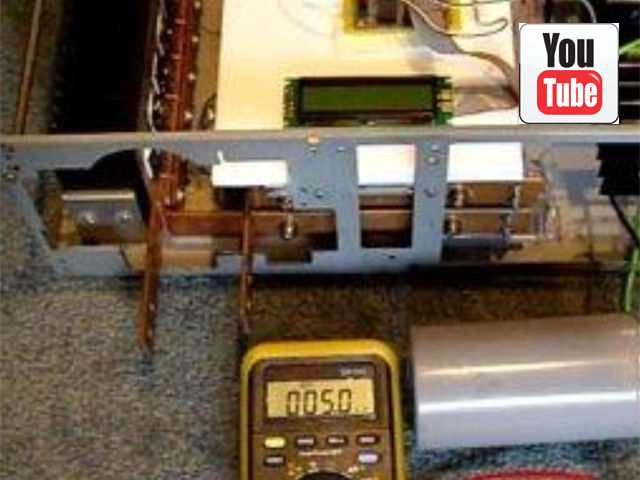
Movie 1. Stuff Starting to Work
While my design is a one-off, I have been cognizant of the need to remove any module for servicing, adjustment or modification with relative ease. I have taken care in the layout of IDC connectors to ensure that the processor board can be readily removed for reprogramming, and that that any circuit module can be rapidly electrically disconnected without soldering (with the exception of the weld discharge board - a matter of matching convenience against circuit performance). This has required the use of screw terminal blocks. While these are low cost, alignment of fine conductors can be difficult, their connections get mangled after just one use and individual conductors are often cut (even under hand torque). The solution to this problem is to solder a piece of used solder braid to any fine wires. While there is a potential long term issue with solder creep under pressure this method allows you to make re-useable and reliable fine wire connections in screw terminal blocks.
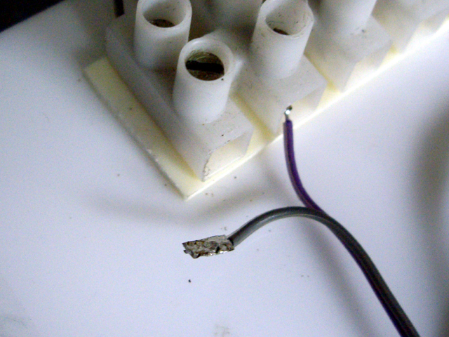
Figure 22. Fine Wire Screw Terminal Block Connection
In my haste to get my welder working using an existing chassis I have not been as considerate of physical mounting as I have been of electrical connections. There are now almost one hundred 3 mm nut and bolt connections for hardware mounting (and a few larger ones) that, while relatively easy to undo, are difficult to make. This aspect of the design needs refinement in a kit set - primarily by the use of taped holes as opposed to nut and bolt connections. I will persist with the problems that I have made for myself.
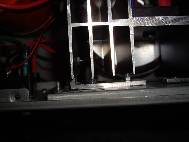
Figure 23. A Stupid Place to use Nuts and Bolts (silly me)!
Wiring colour (or color) coding is really important on a project like this. Ensuring consistent and appropriate colours on high current, high voltage or safety wiring is essential. However this is not practical when you have many many low level signals. My advice is to be as colour consistent as you can and, when you can’t use multicoloured ribbon cables, use coloured heat shrink sleeves so you don’t end up plugging stuff together the wrong way around.
My final thought for this evening (make that this morning) is some form of soft-start for the welder. Have you ever heard a ‘clunk’ when you’ve turned stuff on and perhaps blown a fuse? The residual magnetic field in transformers and the mains cycle at the time of switch on are a likely cause. Limiting mains current for a few cycles, or zero voltage switching are solutions to these problems. Hey, I haven’t blown any fuses yet so this is a potential future refinement.
24 November and after extensive testing to ensure no possibility of over-voltage I have wired up the main discharge capacitors on to bus. I was surprised by how fast they charged so I set about measuring their capacitance. At a constant charge current of 0.614 A they charge from 0 to 15 V in 17.25 s. The relationship between capacitance, current, time and voltage is well established:
F = A * s / V
This means that the actual capacitance of the Boss CAP2S capacitors rated at 2 Farads and a maximum DC voltage of 20 V (24 V surge) is actually around 0.34 Farads. This makes me feel rather angry and ripped-off. How can a company market a product that performs at one sixth of its stated rating? I have written to Boss Audio about my concerns. They have yet to respond and somehow I don’t think that they will. I strongly recommend that you avoid Boss capacitors for your welder - and if this is indicative of their products and quality control then maybe you shouldn’t purchase from them at all. Fritz has posted some capacitor test information that indicates good performance from the Rockford range of capacitors (at or over specification and very low ESR). I am quite happy to destroy these Boss capacitors in my testing because they are rubbish. I am going shopping.
25 November and the resistors and rotary encoders have arrived. The resistors went straight into the charge and discharge boards which are now happily charging and discharging the under-specification Boss capacitors between 10 and 15 V in less than a second (more evidence of their lack of capacity). Because the capacitance is so under-specification there is now some overshoot on the charge and discharge cycles. This is because a single 15 ms 10.2 A current pulse is causing significantly more than 0.1 of a volt charge/discharge.
Another effect of the under-specification capacitors is that the power-down discharge cycle is not as effective as I would like. Using:
F = C / V
the charge on the power supply capacitor is 0.047 F * 26.4 V = 1.24 C. When we distribute this charge with the fully discharged weld capacitors we get 1.24 C / (0.6 F + 0.047 F) ~ 1.9 V. If the capacitors were actually 4 F then the power-down sequence should result in 1.24 C / (4 F + 0.047 F) ~ 0.3 V.
The good news is that nothing is getting unduly hot operating at the design current however the charge and discharge heat sinks are getting warm to touch after a few minutes of continuous charging and discharging.
26 November and I have managed to track down some new 2 F capacitors sold by Jaycar Electronics with the Electus brand name ‘Response Precision’. I purchased them on the understanding that if they were more than 20% below rating I would be returning them. One was marginal at 1.6 F. The other failed at 1.45 F. There is another problem with these capacitors. They have some form of internal current and voltage regulation (beyond all the usual stuff that they stick on the top like LEDs and a voltmeter). They will be going back to the shop tomorrow. This capacitor bother is going to cost me at least another week on my timeline - when I expected to be making sparks this weekend. Boss is not my favourite brand just now.
Looking on the www I have found that Quantum Audio capacitors come with a maximum specified ESR and a tolerance band for capacity of -10% to +50%. Rockwell Fosgate also appear to make a fully specified 2 Farad product but with a reduced maximum voltage of 18 V, and they are somewhat more expensive than Quantum Audio offering. I am trying to purchase some Quantum capacitors but the suppliers I have found seem to have problems with shipping to clean, green (and non-threatening) New Zealand. I will keep on trying.
Time to test the rotary encoders. Now that they have arrived I can see that I will definitely need to make another PCB for mounting these behind the front panel, probably combined with the LCD and my little piezoelectric buzzer (which I should have put on the processor board). They kind of work but increment and decrement in steps of 0.2. most of the time (this should be 0.1). I suspect that this is a straight forward software problem associated with additional interrupts from switch noise - a matter that I will attend to tomorrow. The encoders also have some LED lighting and a switching function that I have not utilized in my design. I will make provision to use these features with the auxiliary IO ports once I have figured out how they work.
With all of this testing the charge and discharge heat sinks are starting to get warm. The temperature sensors are currently mounted as far away from the fan as possible but they should be mounted closer to the power semiconductors on the thickest section of the heat sinks. I need to revisit this.
While a 10.2 A charge and discharge current is fine for testing it is just 2/3 of the transformer rating and we (you and I) want to be able to complete the next weld in the minimum time and we might also want to do some plasma cutting. I can’t wait another two weeks for more resistors so I may incorporate a third parallel resistor on the existing boards.
So close and yet so far!
26 November and I have refined the rotary encoder software routines so they operate as smoothly as possible but there is still a very occasional several digit jump. When I make the mounting board I will incorporate 3 ms of hardware de-bouncing with external pull-up resistors (the programmable MCU IO pull up resistors have a significant tolerance band of between 20K and 50K Ohms).
In my testing today I reduced the charge and discharge pulse widths to 5 ms to avoid overshoot and subsequently identified another fault with the Boss capacitors. The maximum DC voltage they will reliably withstand is about 18 V and this drops as the temperature increases. These capacitors are rated at 20 V with a 24 V surge and I have not applied more than 20 V to them! So when I wind the charge voltage up to say 18.5 V the charge circuit comes on and stays on delivering 10.3 A to the capacitor bank which will not accept further charge and consequently starts to get warm (positive feedback) as does the charge circuit heat sink. I reiterate that these capacitors are rubbish. I will be cutting them open when my replacements arrive to find out if they have active circuit protection in the can.
So where am I at?
- The charge and discharge boards are working reliably but the current needs to be increased by addition of a further parallel current sense resistor. This is not a priority because of the abysmal performance of the Boss capacitors.
- I need some new capacitors urgently. Hopefully these will ordered tonight. This stretches out completion of the welder by perhaps two weeks.
- The temperature sensors are working reliably but need to be mounted closer to their respective power semiconductors. No urgency here either nothing is getting so hot that I can’t put my hand on it.
- The rotary encoders are working but need some hardware de-bouncing for truly smooth operation. Making the board is my next mission.
- The pulse board drive have been tested into rated load and works well but it needs to be mounted for in-circuit testing.
- The discharge electrodes need to be made.
The clock has just struck midnight so here is the update for yesterday, 27 November. The control board is made, connected and tested (Figure 24). This is not the greatest board design that I have produced because it really needs to be double sided for optimal lead alignment and ease of soldering. However it is functional. Note the Perspex temporary mounting plate. Remember that while the case is grounded it might be up to 20 V above the negative rail and I don’t want to do any more inadvertent welding.
The additional hardware de-bouncing on the rotary controllers works well and there is no digit jumping apparent on any control. A single full turn adjusts any setting by exactly 2.4 in 0.1 unit increments. In essence these are performing as 10 turn potentiometers. They feel great and an 0.1 unit adjustment is easily made without any jitter.
I have made allowance to utilize the push button switches and the red and green LEDs on the rotary controls but I have not used these as yet. The controls are on 1” (25.4 mm) centres (copied from the control separation on my oscilloscope - you can be assured that Tektronix got this measurement right).
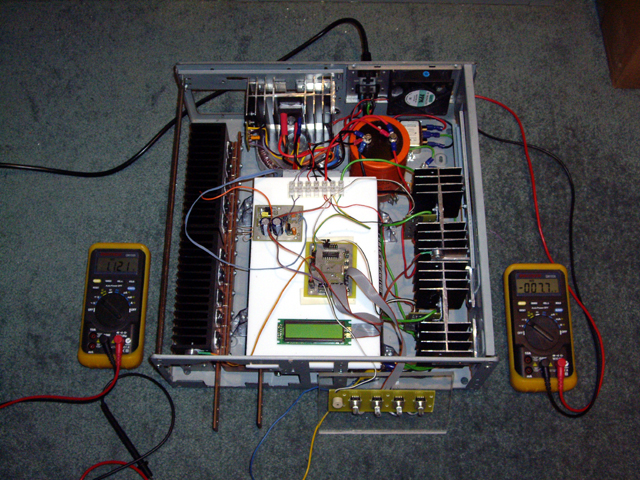
Figure 24. Control Board Fitted
My replacement Quantum Audio main discharge capacitors are on order. They cost a little more than Boss’s paper weights, but are substantially cheaper than the Electus ‘Response Precision’ or the Fosgate 2 Farad capacitor. Hopefully these will be up to specification, otherwise I will be making a capacitor bank using computer grade screw terminal capacitors - and this may result in problems with case size. Hopefully I won’t need to go there.
Oh, and I have purchased a foot switch rather than making one from scratch. A steal at $NZ30 although I may have to replace the cable with shielded cable to reduce the risk of noise pickup.
28 November and those under sized capacitors take about 5 ms to charge or discharge 0.1V at 10.2 A (4 Farads should take about 39 ms). This means that even with the reduced charge/discharge pulse the main discharge capacitor voltage essentially tracks the set voltage and as a consequence the weld-ready buzzer signal sounds continuously when a voltage adjustment is made. The easy fix is to incorporate a delay that inhibits the weld ready signal for about 1 second any time the capacitor voltage is adjusted. I’m adjusting the software to implement this.
The First Sparks (Controlled Discharges)
The weld pulse board has been fitted and I have carried out some initial controlled discharges. My first experiments were with a 100 mm length of 0.38 mm diameter copper wire (4” x 0.015”) twist tied across the buses (lets call this a standard bridge wire for future reference). I got some lovely sparks at the twist-tie connections and a nice red/orange glow down the copper wire with CVSet = 12V, Pulse 1 = 2.5 ms, Dwell = 2.5 ms and Pulse 2 = 10 ms. The wire eventually melted as the Pulse 2 duration was increased.
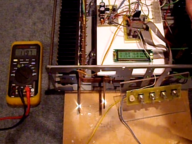
Figure 25. Sparks under Controlled Discharge Conditions
Things were happening fast (in milliseconds) so I replaced the bridge wire with an 0.12 Ohm resistor so I could measure the pulse duration’s and current with my oscilloscope. At 13 V I was getting clean, perfectly timed 75 A pulses (the current was down a bit due to the clip lead resistance) and all of the controls were working faultlessly. But at 15 V, while the pulse timing remained good with 105A pulses, the discharge circuit was oscillating after Pulse 1 (see Figure 26).
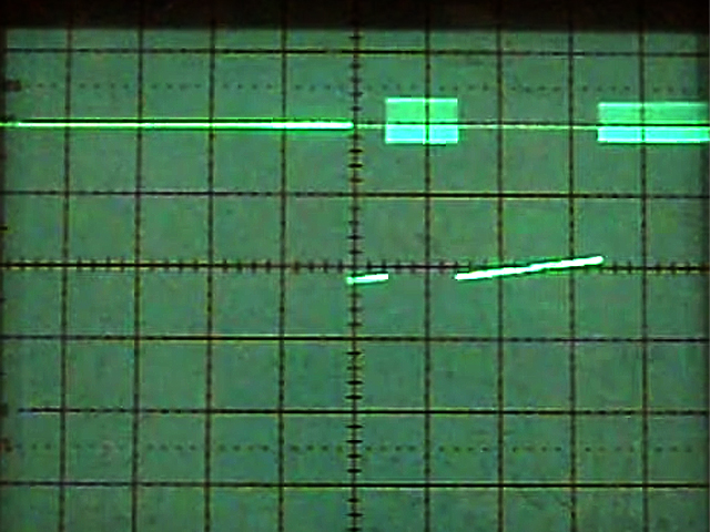
Figure 26. 15 V CVSet. 105 A discharge.
Pulse 1 = 2.5 ms, Dwell = 5 ms, Pulse 2 = 10 ms.
At 14 V (and up) the initial discharge was causing a sustained oscillation of slightly over +/- 1.5 V at approximately 1 Megahertz after the initial discharge pulse (Figure 26) . This stopped immediately if the buses were shorted or were made open circuit (conditions that can be expected to occur during welding) so the oscillation is not a fatal design issue.
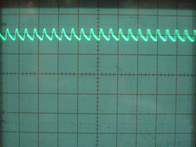
Figure 26. Oscillation at Approximately 1 MHz across 0.01 Ohms.
My first thoughts were that the instability was being caused by a ground loop through the oscilloscope, or power supply glitches affecting the microprocessor. These have been eliminated.
Observations: There were are no oscillatory problems with the twist-tie copper wire at any settings. During oscillation the charge and discharge boards are getting hot so these are on - probably as a consequence of the normal charge and discharge cycles trying to compensate for the oscillation and consequently providing the energy and transients to sustain it. The currents associated with the oscillation are about 10 A - consistent with that the charge and discharge circuits operating.
Through successive ground loop elimination the problem appears to have been a ground loop in the negative rail of the main discharge MOSFET gate control circuit. This has been eliminated and circuit operation is now stable under open circuit conditions, with the 0.12 Ohm load resistor and with a bridge wire. (Note: the actual problem was later determined to be with the Boss capacitors as they progressively failed.)
Figure 27 shows a 17.5 V discharge with Pulse 1 at 2.5 ms, Dwell time of 2.5 ms and Pulse 2 at 10 ms across a bridge wire. A subsequent pulse with the same settings on the same wire caused the bridge wire to fail with the centre section being vaporized (Figure 28).
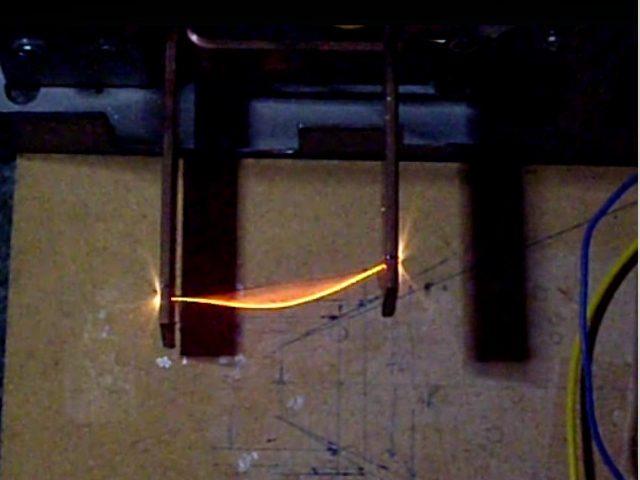
Figure 27. This actually looks capable of making a weld.
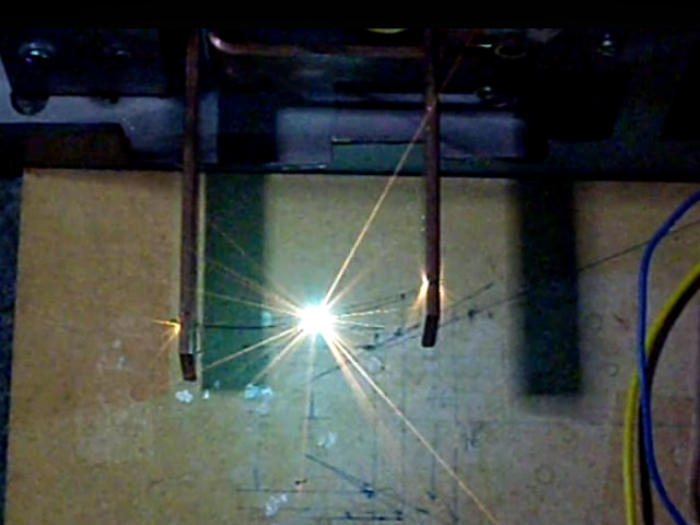
Figure 28. Nuking a Bridge Wire
(Not to worry, there is no damage to the welder or the buses and I had my safety glasses on.)
And nothing, other than the 0.12 Ohm test resistor and bridge wire is getting hot. Figure 29 shows just how hot the test resistor is getting. The helical resistance wires are actually heating up and glowing through the fired vitreous enamel (after repeated discharges the enamel failed and the resistor burnt out open circuit). Neat! I must apologize for the quality of these last few images. The pulses are of such short duration I’m having to make videos and clip to the relevant frame.
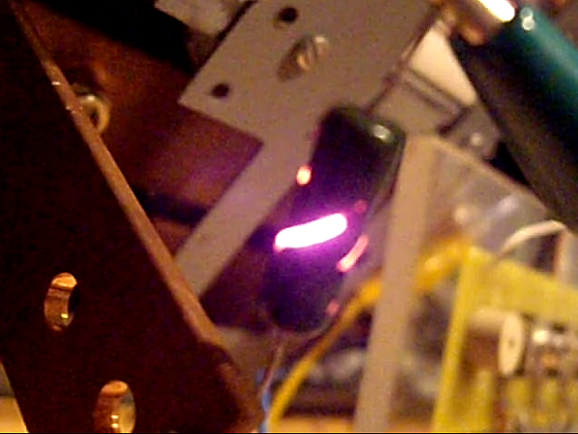
Figure 29. 0.12 Ohm 6 W Resistor Not Enjoying about 150 A!
Enough sparks for now. I need to get on and make the weld electrodes, sort out a front panel so I can mount the controls and LCD display, and mount the MCU and processor board with something more substantial than double sided adhesive tape.
29 November and the electrodes and cable assembly are about half made. A drawing of my construction is shown at Figure 30. I have no idea of the optimum angle for the weld probe tips - these will require some experimentation - but they will wear over time so they need to be removable for sharpening or replacement. At this stage I have made no allowances for using tungsten tips or other, more exotic, materials for now. If (when) I get there I will probably shrink fit these in the existing tip design for good thermal and electrical connection and grind the tip profile.
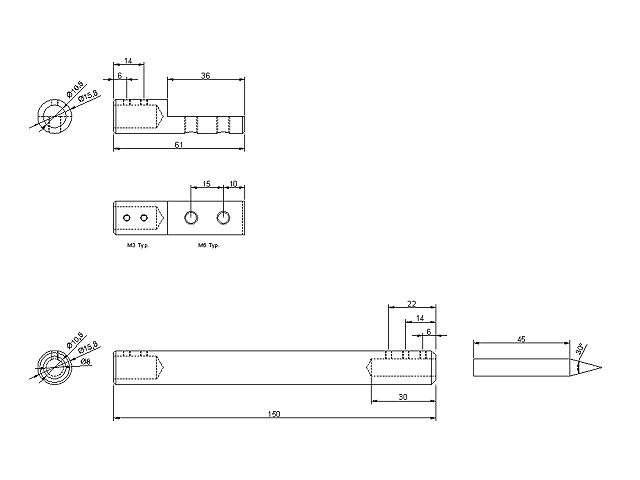
Figure 30. Lead Set Concept
With my braided 0G cable I have found that once the insulation is removed the stuff splays all over the place making it next to impossible to insert into the mating recesses. My initial solution was to lightly solder the end of the cable with the insulation still in place, then strip the insulation and if necessary lightly hand file to remove any excess solder. A better solution is to use a rubber band!
I intend using M3 grub (set) screws to hold everything together. The grub screw cable connections are not compressing the cable against the shell as with a standard terminal block. The grub screws actually fill the void, forcing all of the braids together and into contact with the shell. This should produce a physically and electrically robust connection. If necessary to achieve a really tight fit add some brass shim or a few additional strands of copper wire.
I have found some white Perspex for the front and rear panels. Rather than drilling mounts through the panel I intend to glue M3 studs into the back of the panel for a tidy finish. The front panel requires 6 through-holes, 12 studs, and milling of a rectangular cut out for the LCD display and the two slots for the electrodes. The back panel has 8 studs and the fan, fuse and power connection cut outs. I have some marking out to do!
There are a few further design improvements that I am contemplating.
- Optimizing the connectors. The current design works, with every module readily disconnected, but this could definitely be improved. A lower connector profile with a more positive fit would be preferable.
- Incorporate additional power supply filtering on the charge and discharge boards. There is none at the moment and I suspect that this may well have been a contributing factor to the negative rail oscillation.
- Put the fan under processor control (it is currently connected directly to the 12 V auxiliary power supply on the pulse discharge board but the processor is measuring the temperature at least 250 times each second). Why cool stuff when it doesn’t need cooling.
- Start writing the plasma cutting routines and incorporate these in the code. This should be easy with just three parameters to consider - CVSet, Pulse and Dwell. The top level flowchart is: If the foot switch is on then repeat: fire a pulse and dwell. Charge to maintain to CVSet. I’m sure it will end up being more complicated than this.
For your interest I am up to Version 6 of the code. It comprises 1,744 bytes of instructions, 1,436 bytes of data, and 290 bytes of EEPROM space consuming about 2.5% of available memory assets. There is ample space for code extension should this be necessary.
30 November and the lead sets are done as shown in Figure 31. A couple of the grub screw holes aren’t exactly on centre which is rather annoying but I only have myself to blame for lazy machining practice (the marking out was good). However they should be functional and I want to get welding sometime soon. The probe design may need some refinement anyway - but I won’t know until I get to weld something. I’ve completed a few more bridge wire tests through the leads and everything appears to be in order. The only tricky bit was machining the probe tips for a close running fit in the handles. As I don’t have laps or hones I settled on 0.05 mm clearance and some polishing of the probe tips.
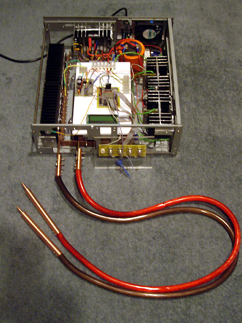
Figure 31. Lead Sets Assembled and Connected
Tomorrow the foot switch gets installed and I hope to make a start on the front panel.
1 December and the foot switch was rewired with a shielded cable (an old computer keyboard cable) as shown in Figure 32. The plug socket (a panel mounting three way audio jack) has two uncommitted switches on it which has allowed me to incorporate a test for the presence of the foot switch on power up and provide an appropriate warning on the LCD. I also remade the probe cable connections using brass shim under the set screws, The feel as I tighten them is far more positive than my earlier arrangement. Finally the copper main bus termination’s were cleaned to ensure a decent low resistance connection.
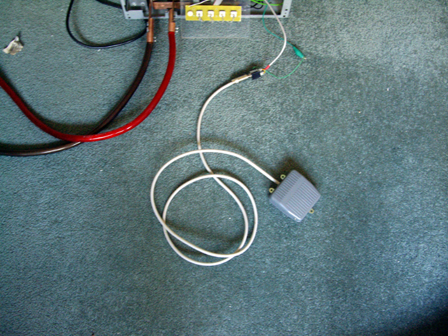
Figure 32. Foot Switch
No time for the front panel today - I want to get on and start making some welds. The very first effort was with an 0.65 mm diameter copper wire cross. There was a spark and the wires had blown to bits. Either not enough pressure, poor pulse timing or too higher voltage. I turned everything down and tried again but with limited success - I got a weld but it was very weak and pulled apart. I put the voltage back up a bit and tried welding a zinc plated machine screw to brass shim. The first attempt blew a hole through the shim. I tried again with more pressure and got a weak weld, but both the brass and the screw had definitely melted. Next I tried a piece of copper wire to brass shim. Again a weak weld even with the pulse time extended.
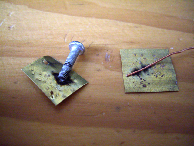
Figure 33. Weak Initial Welds
I also tried brass to brass but no weld occurred (and I managed to make a heap of holes). My final experiments for today were with some of the studs that I built this thing for. While I definitely got welds they were simply not strong enough. With some effort the studs pulled off the stainless steel as shown in Figure 34.

Figure 34. Poor Stud Welds
There was virtually no electrode sticking throughout these initial tests which, with the poor weld quality, suggests that the energy levels are way too low. The welder itself performed faultlessly with no instabilities apparent, nothing getting hot, and the probes remained nice and cool.
I suspect that the primary issue is a lack of main capacitor charge (those lousy Boss capacitors again). The available energy is about a tenth of the design value. The initial pulse depletes the charge significantly and there is insufficient energy left to get the work pieces truly hot and forming a nice weld during the second pulse. If I wind the capacitor voltage up I tend to get big sparks and loud noises - neither of which are desirable. If I cut the Dwell time to zero the software makes a single pulse for the duration of Pulse 1 and Pulse 2. However increasing the duration made no perceivable difference to the welds above nominal settings.
A secondary issue is clearly to do with my technique. I need to experiment further to get the pulse timing, pressure, voltage and polarity right. Apparently this is referred to as developing weld schedules. Some commercial welders can store these in memory - another refinement perhaps?
I have looked around the Internet for some advice on these issues. Apparently the primary pulse energy should be between a quarter and a half of the secondary pulse. If the voltage is too high and/or the pressure is too low then expect sparks. On polarity, it appears that I need to make the more resistive or thinner material negative, but that this will also result in uneven electrode wear. I have no guidance on the dwell time between pulses but I suspect from a discharge oscillogram on the web that this should be around 10 ms.
2 December and I have incorporated the ‘foot switch disconnected’ warning. A word of caution about the selection and wiring of the plug and socket. Because the switch, cable and plug are shielded at ground it is important to ensure that there is NO POSSIBLE contact between the negative rail and ground during insertion and removal of the plug. This allows hot connection and prevents inadvertent welding of the socket to the plug.
I drew up the front panel today and realized that I can’t make this until the new capacitors arrive because they may influence the position of the upper electrode connection. I need those new capacitors like yesterday!
I’ve also been thinking about potentially better ways to make those stud welds. Rather than simply making a number of welds around the flange of the stud it would be relatively easy to make a point contact weld. This requires a dimple on the mating surface of the stud, which is really easy to machine by having a lathe facing tool slightly off centre, and a recessed positive probe tip to ensure good electrical connection to the top of the flange. When the weld pulse fires the dimple vaporizes making a hot ionized path for the second discharge while the stud is being pressed into the developed molten pool. The theory sounds good. More experiments are required.
Measurement Day (3 December 2011)
Time to investigate the performance of my welder in a more systematic way. If you don’t do maths then maybe you want to skip some of this bit.
The first item that I need is a high wattage low value resistor. I have some Nichrome heating elements with 0.43 mm diameter wire having a resistance of about 8.68 Ohms per meter. By placing three stands in parallel, twisting them together (which increases the required length of each strand by about 5%) and connecting the welder across just 10 mm I have a nice 0.029 Ohm resistor sample resistor (within about +/- 20%).
I set the welder to CVSet = 10 V, Pulse 1 to 5 ms, Dwell to 3 ms, Pulse 2 to 15 ms. The scope was set up at Vert. 5 V/div , Horz. 10 ms/div and the probe directly across the test resistor. With the video running I fired a few welds, allowing time for stuff to cool a bit between pulses otherwise the resistance of the Nichrome would increase appreciably as it got hot (Figure 35).
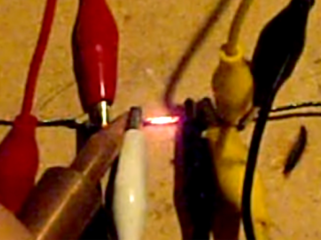
Figure 35. Test Weld Pulse Set up
From the video I calculated the current through the test resistor at the beginning of Pulse 1. From Ohms law: I = V/R = 7 V / 0.029 Ohms = 240 A. The lead-loss for my experimental set up was calculated as 0.012 Ohms which is almost entirely due to a triple clip lead connection, a necessary evil because I only have two hands and one foot switch.
The discharge curve at Figure 36 shows a nice exponential decay. Using V = Vo e-t / RC, and knowing Vo, V, t, and R, the capacitance can be calculated as 0.31 F. This is interesting. I suspect that one of those Boss capacitors has failed because this is half of my earlier measurement of the parallel capacitance value based on constant current charge time. This also leads me to suspect that the oscillation that I experienced earlier was also associated with the imminent failure of one of these capacitors. I have remade the negative rail connection to the main MOSFET driver board, duplicated the earlier oscillatory conditions and tried a wide range of resistive loads with absolutely no instability. Please forgive my repetition but these Boss capacitors are garbage. Although I have now posted several tickets with Boss they have not replied. So much for customer service and confidence in the quality of their product!
It is apparent from the curve at Figure 36 that heating of the sampling resistor has had no appreciable effect on the measurements.
Using Excel I set about modelling the performance and overlaid this (red line) on the actual measured discharge voltage across the test resistor. I also overlaid the expected performance of a 4 Farad capacitor (blue line). See Figure 36.
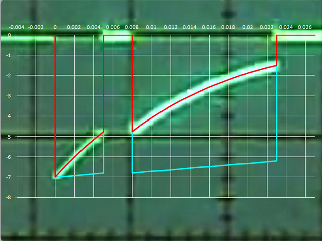
Figure 36. Discharge Measurements.
Graphic Overlay: Horz. 2 ms/div. Vert. 5 V/div.
You can see how closely the theoretical curve models the actual performance, and you can see from the blue line how the circuit should be performing with a 4 Farad capacitor. Note that the pulse and dwell timing remains absolutely spot on under microprocessor control with nice fast transitions and absolutely no over-shoot.
The delivered energy in the pulses can be calculated by integrating the delivered power over time. This can be done by linear approximation, numerical integration, or completing the indefinite integral. The former methods tend to over estimate the delivered energy so I persevered with the maths (actually not that difficult but note that I have not included the effects of discharge path inductance):
The mathematical solutions are summarized in Table 1.
You can see immediately that with the existing capacitors there is very little weld energy left after the first pulse even though this is just 5 ms duration. This explains why my experiments with increased pulse width were having very little effect. As expected there was nothing left to discharge.
The energy required to heat just 1 cubic mm of steel to melting temperature, assuming no heat dissipation, is approximately 11 J. If you take into account the various resistance components in the discharge circuit (there are a lot of contributing series elements but the dominant ones are the capacitor ESR, probe to work contact resistance, and the weld junction itself) then it is not surprising that my welder can’t make real welds yet.
There are a number of commercial CD welders that use programmable energy (in J or W s) as an input parameter for making welds. The reason for this is that weld energy is not linearly dependant on the capacitor voltage (see the equation above) but on the square of the capacitor voltage. The dependance of delivered energy on weld path resistance is highly non-linear as shown in Figure 37 and it is difficult to predict as there are many relevant variables in any given weld. (You can calculate this dependance explicitly as dE/dR using the function of a function rule but this took too many pages of my design notebook to complete and validate to publish.) In any case the real weld resistance is not static but can be expected to change significantly as the weld progresses. As most metals heat up their resistance increases. Interestingly when metals melt their resistance is about twice that of their resistance just below the melting point, but the contact resistance also decreases to nearly zero through this transition.

Figure 37. Delivered Energy as a Function of Weld Resistance
(25.5 ms Single Pulse, 4 Farad Capacitance)
I have estimated the discharge path resistance, considering parallel and serial terminations, MOSFET on resistance, the conductor resistance’s and capacitor’s ESR (less contact and weld path resistance) to be approximately 0.003 Ohms. The maximum change in main discharge capacitor voltage, dV/dt, which will occur at a CVSet of 20 V at the start of a pulse is therefore Vo / RC = 20 V / (0.003 Ohms * 4 Farads = 1,667 V/s at a current of 6,670 Amps. To ensure 0.1 V resolution we would need to make make ADC conversions in 0.6 us with at least 8 bit precision. Aside from the noise issues associated with taking ADC readings during a relatively high current pulse this simply isn’t possible with my current processor and clock rate.
I figure that the commercial welders simply display percentage potential weld energy:
as opposed to actual delivered energy which removes the dependance on the value of the discharge capacitor, resistance path and pulse time. This is well within the capabilities of the ADC at 256 bit resolution and can easily be implemented using a look up table. The rotary encoders make linear operation a breeze. I might yet implement this.
The project is on hold for now until the new capacitors arrive. Not to worry - I have a million and one other things to be getting on with.
5 December and I have heard back from Boss Audio! The fact that they have responded at all is amazing. The fact that their two email responses were lodged in my SPAM account was also appropriate. Their responses from a ‘no reply’ address did not answer my questions and simply referred my request for a refund to the retailer. I assume from this that Boss sell a lousy product, are completely aware of this, and on the basis that most consumers will not know the poor quality of the Boss products they have purchased, they will continue with their current business model to ‘reap while the sun shines’. Please purchase Boss Capacitors if you want an ineffective welder or a sub-standard audio capacitor for your mega-boom sub-woofer car audio sound system. And don’t be surprised if the transients cause the Boss capacitor to fail and burn your lovingly hand-polished pimp-mobile to an ugly charred shell of distorted steel, voiding your insurance because this was probably an undeclared modification to your vehicle’s electrical system.
As an aside I have decided to reduce the maximum charge voltage on my new capacitors (when they arrive) to 18 V. Although they are rated at 20 V this is their maximum and stressing components to their limits is something to avoid if at all possible - particularly when temperature rise can be expected to degrade performance.
I have also had some time to reflect of the design of my weld probe tips. At the moment they are needle point sharp with an inclusive angle of 30° as shown in Figure 30. While this ensures excellent probe pressure (a function of force over contact area) it also means two very small conductor diameters in the discharge path which results in power dissipation and rapid erosion of the probe tips. I suspect that a secondary cut at say 45° will retain an appropriate weld pressure while ensuring good electrical contact and improved minimum probe cross-sectional area. We are, after all, trying to heat the weld junction and not the junctions between the probes and the materials being welded. This should have the advantages of reduced heating and erosion of the weld tips, increased probe contact area and reducing probe stick. There is a lot to probe tip design that I know nothing about and I am certain that there are reasons why companies like Weller make a whole range of tips for their soldering stations.
My final thought for tonight is another construction note. The MOSFET leads in my charge and discharge circuits and the main pulse discharge circuit require forming to make the connections (see Figures 11 and 20 above). Do not bend the MOSFET leads right by the case, use fine-nosed electronic pliers, allow for some bend radius (at least three times the thickness of the lead), do not repeatedly work the bends, and do not force the connections. There are a lot of ‘do not's’ here but if you you choose to ignore these then you risk lead failure or increased lead resistance, neither of which is desirable.
6 December and my new capacitors have arrived, been tested, and I am negotiating how to return them. They measure up using low current resistive charge and discharge techniques at just 0.3 Farads each. Cross Quantum capacitors off your Christmas card list.
I set about continuing my experiments with the Boss capacitors using low charge voltages between 8 and 12 Volts, and short pulse durations of Pulse 1: 2 ms, Dwell: 0.1 to 2.5 ms, and Pulse 2: less than 9 ms. The weld was an 0.65 mm copper wire to a plated steel washer. The positive probe was placed firmly in contact with the washer and negative probe was used to press the wire against the washer. The distance between the probes was about 5 mm. Occasionally I got big sparks with significant erosion at the positive electrode. I suspect this implies poor electrical contact between the positive probe and the washer. While almost all of the welds above 11 Volts stuck none were what I would call secure.
After about the 70th weld the welder suddenly became permanently in trigger mode - so that when I applied the electrodes there was an instant (and significant) spark. The LCD control panel showed no error, and the temperature of the charge heat sink was just 27°C with the weld heat sink sitting just above ambient. I reset the unit - all good including a test of the foot switch, and set about welding at the same settings but the unit was still triggering continuously. On about the third attempt one of the discharge board MOSFETs literally exploded (Figure 38). Bugger me! (I recognize that this is a potentially offensive phrase, but here in God’s Own it is a colloquial expression of surprise).
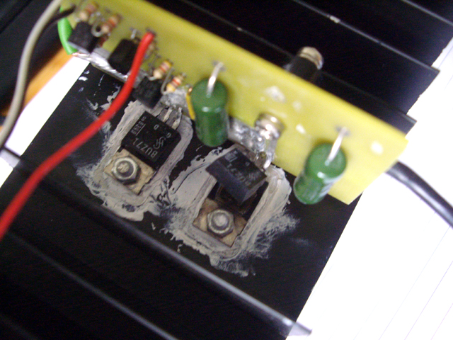
Figure 37. MOSFET on the Discharge Board Literally Exploded
My first mission was to de-energize the unit and disassemble the discharge board and get rid of those jolly Boss capacitors. With the modular construction this took just 15 minutes.
I measured the capacitance of both Boss capacitors at about 0.24 Farads each (even lower than when they were first installed). With my trusty hacksaw I carefully cut the top off one. It was immediately apparent that the pitch encapsulation inside the can had locally melted and that the liquid electrolyte was sloshing about above the pitch seal (Figure 38).
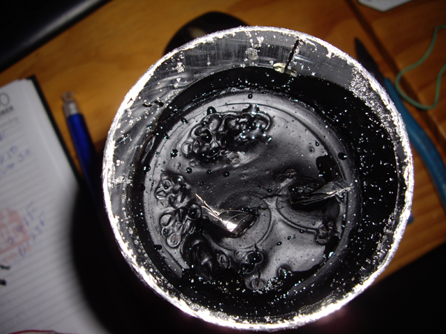
Figure 38. Localized Pitch Seal Melting with Insulation/Dielectric above the Seal
(The white speckle is aluminium swarf from hacksawing.)
The liquid smelled like burnt oil - not good and probably very unhealthy even through it was probably a solution of sodium borate in water with additives and pitch volatiles. I proceeded to wash the capacitor in toluene followed by water to get rid of the evil liquid and then sectioned the capacitor. Interestingly the actual capacitive element was not central to the case but had tilted in the pitch during manufacture - almost coming in contact with the aluminium case. Its overall dimensions were just 41 mm diameter by 75 mm long (in a case 76 mm in diameter by 215 mm long). There was some type of refractory block in the base of the capacitor that smelled strongly of ammonia and dulled my hack saw blade at the speed of light. See Figure 39. As expected the capacitive element contained rolled plates of etched and oxidized aluminium with paper insulation, both approximately 0.04 mm thick (Figure 40). I strongly suspect that the other capacitor is equally crippled due to insulation/dielectric release based on my external measurements. Anyone that buys one of these capacitors might reasonably ask why they are paying for 1/3 brick, 1/3 pitch, and somewhat less than 1/3 under specification capacitor!
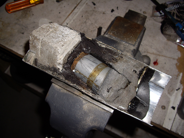
Figure 39. Sectioned Boss Crapacitor
(Note the small size of the capacitive element relative to the can and its strange angle.)
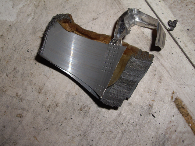
Figure 40. Layered Aluminium Capacitive Plates and Paper Insulation
So now all I need to do is work out what went wrong and what else is broken. This will probably take a day or two.
7 December and the first problem and a probable primary cause have been found. The reason the foot switch had become inoperable (always on) was that one of the main MOSFETs had failed - dead short between all three electrodes. And the reason? This particular device was the one over the heat sink plug. I don’t think that this was a coincidence. The plug was about 0.05 mm proud of the heat sink surface so the MOSFET cannot have been in good thermal contact with the heat sink and consequently got too hot (after 70 or so consecutive welds). The problem has been fixed by hand scraping the plug dead flat with the heat sink surface, replacing the dead MOSFET, and finally cleaning and reassembling the bus structure. Now is a good time to move the thermal sensor too. Done! My mechanical bus structure really helped with identification and replacing the dead MOSFET. This would have been a real trial had they all been soldered in parallel.
What else is dead? All of the MOSFETs on charge and discharge boards and their driving transistors. I kind of anticipated at least one disaster of this magnitude and have replacement components already in stock. (Why buy one when they are cheaper in 10 off?) Under normal processor control the charge and discharge boards are never on together or during a weld pulse, but working out the failure mode is a challenge. These high current events tend to cascade with one failed component causing others to fail, and usually very quickly.
I suspect that, after the main pulse MOSFET had failed due to inadequate heat sinking, one of the charge MOSFETs died first while trying to charge the extended output short, rapidly followed by the other and then the driving transistor. Their 150 W per device power rating de-rates at 1 W/°C above 25°C. They failed shorted drain to source so now the full 26.7 V primary supply was being applied to the weld capacitors and the discharge board was trying to reduce the voltage. These MOSFETs are only rated at 40 W per device (no thermal de-rating) so under these conditions they failed very rapidly taking their driving transistor along for the ride.
As a consequence of this failure I have decided to up the power rating of the discharge MOSFETs to at least 150 W per device but it should be noted that the situation that resulted in the failure cascade should not have happened (but for my construction mistake), and even with higher rated components, relatively rapid failure will still result from a similar fault. I can add that the existing MOSFET ratings were specifically designed to be sufficiently power dissipation conservative under anticipated operating conditions.
There is also a software solution that I can apply here too. If, during charge or discharge, the main capacitor voltage does not move about 50 mV in say 15 ms milliseconds then there is a fault with the output pulse circuit, charge or discharge boards. Time to sound an alarm, stop trying to do anything and advise power down and service.
You might ask why I am I sharing my disasters and setbacks with you? Truth is that in developing a circuit like this from first principles (I have not copied anyone else’s design, although I have tried to improve on the work by others) occasionally you will get something wrong with the hardware or the software (and yes - the software can cause the hardware to fail). I know there are other web sites out there with completed welder designs but I haven’t found any that document their development failures. By sharing these issues with you I hope that you can avoid them (a fool learns by his own mistakes - a wise man learns from a fools mistakes) and I also hope to impart some confidence in my final design.
The boards are now rebuilt but I have some more testing to do before reassembly. The main power supply, the processor board, the 12 V auxiliary supply, the control board, the power sense board the temperature sensors and the main pulse bus and associated MOSFETs are good to go. However I still need to test the charge and discharge boards and the weld pulse driver board, and up-rate the MOSFETs on the discharge board. Note that putting components between the processor and anything switching power has paid dividends in my design. Sure, I have destroyed about $30 of components and spent the best part of a day identifying and replacing them, but all of the circuit boards are intact and the main processor board kept on working right up to when I threw the power switch off.
I’m having some difficulty communicating with the supplier of my replacement capacitors. It appears that they have stopped replying to my emails, but for now I will give them the benefit of doubt and assume that they are not receiving them. The cost of sending them back for a refund is significant so I have decided to use these to complete my development anyway. Hey, although they are way under specification they still perform better than the Boss capacitors. Looking at others’ designs I see a few folk have used Volfenhag capacitors. I can expect these to be less than 50% of nameplate so I’ll need to order two 4 Farad devices (to be connected in parallel) in the hope that I can get nearly 4 Farads in the case.
This project is now anticipated to be 25% over budget with at least another NZ$150 for further replacement capacitors and a delay of perhaps two weeks for delivery. This isn’t good but I have gone past the point of no return. The offset is the eventual utility of having the welder and the savings associated with the repair of my still against the cost of replacement.
8 December and everything has been tested, put back in the chassis, wired up and is working. I have increased the discharge board MOSFET power ratings and put the temperature sensors where I should have put them in the first place. This was followed by a series of 240 test discharges with relatively short settings of P1: 2.5 ms, D: 5.0 ms, P2: 8.0 ms, CVSet ranging from 10 to 15.5 V in 0.5 V increments with 20 weld pulses at each setting. The discharge current ranged from about 190 to 300 A. Nothing is getting unduly warm other than my test load (and after the last disaster this assessment included a finger test on every MOSFET in the main discharge array and the capacitors with each voltage change). With an ambient temperature of 22°C the charge heat sink eventually got up to 30°C but I was firing weld pulses every couple of seconds. No signs of oscillation or instability.
I repeated the test that I used at Figure 36 but with reduced lead resistance and a reduced resistive test load of approximately 0.01 Ohms (Figure 41 and 42) using a185 mm length of 0.63 mm diameter copper wire to measure the capacitance under weld conditions. The peak discharge current was just over 1,000 A and the pulse timing was perfect. The parallel capacitance of the Quantum 2 Farad capacitors has been confirmed at 0.6 Farads (as per previous bench measurements) - less than 15% of their nameplate value! From their weight distribution, dimensions and the can finish under the plastic wrap I suspect that there is some ‘badge engineering’ going on here. They appear to be identical to the Boss capacitors and are therefore probably made on the same production line, in the same factory, somewhere in China.
If you look carefully you will see a very brief 1 Volt positive transient in Figure 42 when Pulse 2 switches off. I assume that this is a consequence of switching large currents in short timeframes with inductive loads, but it could also be associated with the ground loop through my oscilloscope. This should not unduly stress the discharge MOSFETs as the body diodes are rated for pulsed currents of 840 A and the capacitors have been discharged by the preceding pulses.
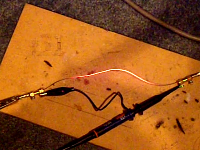
Figure 41. Improved Resistive Test Load (R = 0.01 Ohms) at 1,000 A
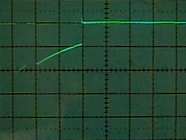
Figure 42. Discharge Measurement. Horz. 5 ms/div. Vert. 5 V/div. Rload = 0.01 Ohms
P1: 2.5 ms, D: 2 ms, P2: 10 ms. CVSet = 13.6 V. Peak current = 1,000 A
I’m about to launch back into the code to reduce the maximum capacitor charge voltage to 18 V, reduce the heat sink temperature alarm condition to 50°C, and to incorporate some hardware failure detection in an attempt to prevent a reoccurrence of my previous disaster.
9 December and the first two code modifications took as may minutes to complete by simply changing three constants in the code. The hardware failure detection took a while longer. The software looks to ensure that the main capacitor voltage changes in the right direction on any charge or discharge cycle by at least 2.5 mV. It has been tested and it works.
With these modifications I can start trying some more welds, but cognizant that the welder is still power-starved due to the capacitors. Weld times were typically P1: 3 ms, D: 2.5 ms, P2: 8 to 10 ms, CVSet: 8 to 12.5 V. I can see why everyone that builds one of these immediately starts welding paper clips to stuff. They seem to weld very well. Figures 43 to 45 show my initial attempts. I also tried a few thermocouple beads but the weld energy was too high and the beads burned off the wire. A note from Figures 43 to 45. You can see that the electrode contact points on the paper clip and the washer and plate show significant melting at the point of electrode contact. These junctions are not where we want to dissipate heat. This is evidence of the need to change the probe tip design to ensure better electrical and thermal contact with the work (more area).
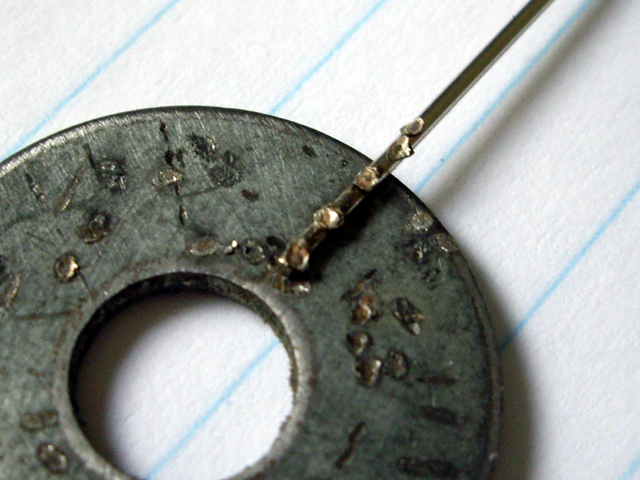
Figure 43. Paper Clip to Washer
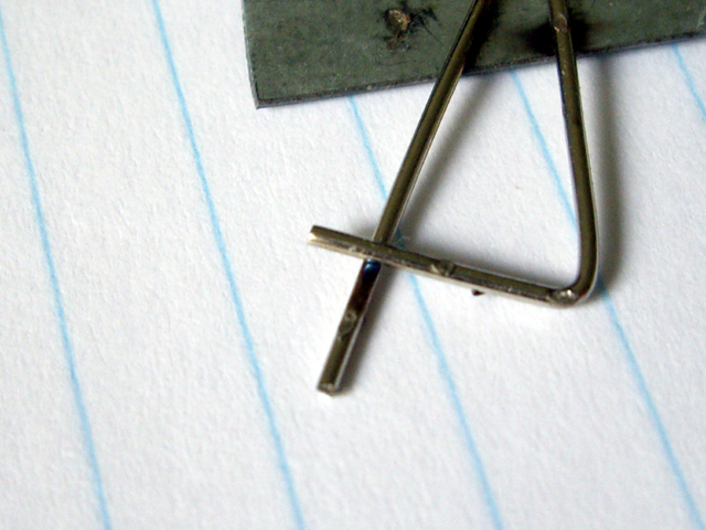
Figure 44. Paper Clip to Itself
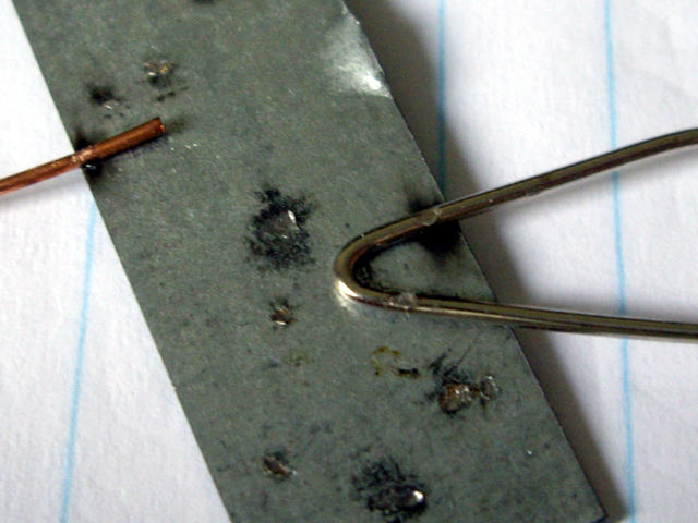
Figure 45. Paper Clip and Copper Wire to Galvanized Steel Plate
Having made these welds (and a few others) I set about pulling them all apart. The paper clip welds were reasonably secure but all of the welds broke before the clip or copper wire. I suspect the problem is the pulse durations are not long enough - but I can’t make them too much longer before the main discharge capacitors run out of energy (see Figure 42). Yes - I need some more capacitors.
A final couple of refinements that I will make are to activate some of the LEDs in the rotary encoders, use their switching function to allow switching to a temperature display (sorry folks this didn’t happen tonight).
I can’t find any 4 Farad Volfenhag capacitors so I have ordered two Rockwell Fosgate 2 Farad capacitors rated at 18 V from Sonic Electronics. These components are significantly more expensive (4 times the cost of equivalently branded products) but Fritz’s web site suggests that this brand will exceed capacitance rating and be within 10% of rated voltage. I have advised Sonic that if these capacitors don’t perform them I will be returning them.
10 December and I have been experimenting with some more welds having put a 45° chamfer on the end of the electrode tips. With P1: 3.5 ms, D: 5.0 ms, P2: 13.7 ms, CVSet: 12.0 V I am getting paper clip to paper clip welds that are as strong as the wire - they simply won’t pull or bend apart. The wire fatigues beside the weld before the weld parts under repeated bending. I am also getting some moderate weld adhesion between my studs and the galvanized steel plate at Figure 45 using the same settings. This is promising because the contact area on the studs was dirty from previous weld attempts, and the welds have already been shown to be substantially more robust with the stainless steel (probably because of its increased resistance). See Figures 46 and 47.
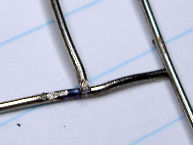
Figure 46. Strong Paper Clip Welds
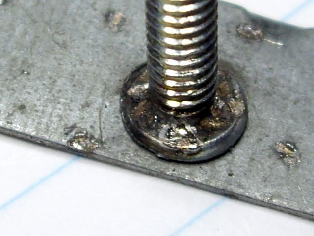
Figure 47. Stud Adhesion
I have designed a concept weld-head for my stud welds. There is little point in doing too much of this until my new capacitors arrive because, with gutsy capacitors, the pulse durations will significantly decrease (perhaps by as much as 50%) and the weld head may not be required.
11 December and I’ve been experimenting with thermocouples. With P1: 3.5 ms, D: 5.0 ms, P2: 15.0 ms, CVSet: 10.5 V I am now getting K Type thermocouple beads that will not pull apart. The trick to my success is the use of a ceramic substrate. Simply strip back about 8 mm of wire, twist together, apply the electrodes with moderate pressure about 3 mm apart and complete the weld. The next progression is to make these welds to a copper disk.
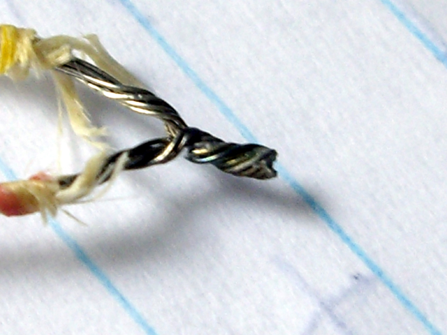
Figure 48. Successful K Type Thermocouple Bead.
(This is as far as it would untwist. The wires break before the bead fails)
Another day - another dollar. It’s just turned 13 December (Black Tuesday?) here in God’s Own and my progress has been stymied but for some real capacitors. I did receive a very helpful email from Mark Sims who has made ‘the CD Welder from hell’ and provided much of the capacitor data published on Fritz’s web site. On the basis of Mark’s advice it looks like my Rockwell Fosgate 2 Farad capacitors won’t make the grade. I have sent a hurried email to the supplier of my latest order in the hope that they can provide a better capacitor. Mark’s recommendations are 1 Farad capacitors by Monster Cable (Intellicap), Rockwell Fosgate and Scosche.
One of Mark’s helpful comments on the need for heat sinks has got me revisiting my MOSFET specifications. His welder has eighteen parallel IRFP2907’s while my current prototype has just ten IRFP3206’s (mainly because this is what I had on hand and all that I could mount on the heat sinks). My MOSFETs are operating right on the Safe Operating Area limits and are dangerously close to the thermal junction limits with just an 0.6 Farad capacitor. Figures 49 and 50 (updated on 17 December) show the relevant design curves so you can see why I am about to increase the number of MOSFETs in my design.
Note that If the Red Line drops below the bottom Single Pulse (Thermal Response) curve then any pulses longer than this are likely to destroy your MOSFETs no matter what the Duty Cycle is. You can also see the maximum Duty Cycle which will ensure that your welder is unconditionally Tjmax stable for any pulse width. Oh, and you can download the Excel Spreadsheet here so you can play with your own design.
As an aside when I designed this stage I didn’t plot out the full curve and nicely overlay it to scale on the data sheet. The three design values that I selected unfortunately missed the critical pulse width at about 1.5 ms (x axis in Figure 49).
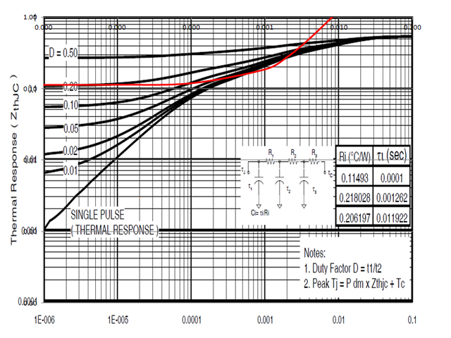
Figure 49. Pushing Ten IRFP3206 MOSFETs to the Junction Temperature De-rating Limit
(C: 0.6 F, Rsd(on): 0.003 Ohms, Rtotal: 0.003 Ohms (meas.), Vout: 20 V)
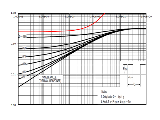
Figure 50. Mark’s Design with Eighteen IRFP2907 MOSFETs.
Unconditionally Stable for any Pulse Width with a Duty Cycle Less that 0.6
(C: 4 F, Rsd(on): 0.0045 Ohms, Rtotal: 0.003 (est.), Vout: 20 V)
I have also been thinking about my probe inclusive angles and contact resistance. As you might reasonably expect the resistance of a tapered probe increases with its length, eventually getting to an open circuit when the taper length provides an infinitely fine point. The theoretical resistance of of an 8 mm diameter 30° included angle copper electrode tip varies with the length as shown in Figure 51. Note the log scale on the y axis. I figure that the probe-to-job connection resistance needs to be significantly less than than the resistance of the weld junction (perhaps by a factor of 10) otherwise I am wasting energy welding the probe tips to the work and heating them up. The other factor here is weld pressure. If the probe tip area is too large then I will struggle applying sufficient pressure to the work.
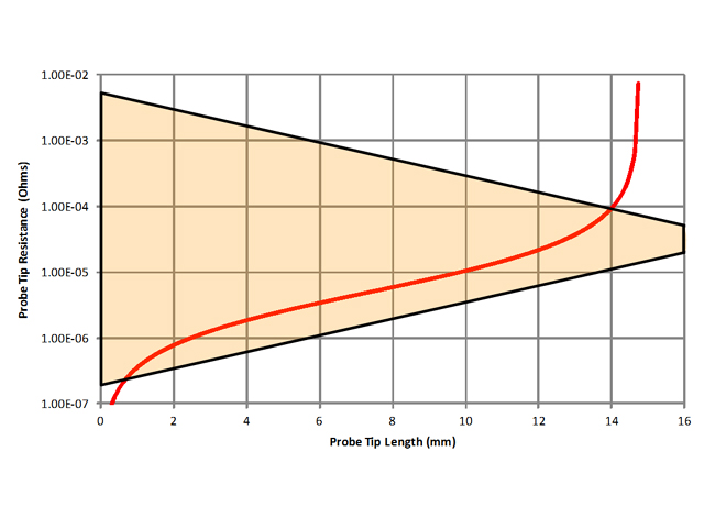
Figure 51. Resistance as Function of Length for a Tapered Probe
(Root Diameter: 8 mm, Included angle: 30°, Material: Copper)
On the basis of Figure 51, I have settled on spherical tip at about 14 mm (that’s 3.5 mm back from the probe point). Another problem with sharp points is to do with sparking (something that I also want to avoid). The increased electrostatic field at a sharp point, or for that matter a sharp edge, is the fastest way I know to reduce spark potentials. These issues may also be a significant contributing factor to tungsten electrode wear that others have reported.
There are lots of postings about the difficulties of getting a good weld to aluminium (for those of you in the good old US of A - you will have to suffer with my spelling and metric units). Years ago I used to solder to aluminium ‘under oil’. Basically get a high heat capacity soldering iron (60 W or more), put a few drops of machine oil on the aluminium, then scrape the surface under the oil, and apply the solder and the the hot iron under the oil. If you’re relatively quick there isn’t even a lot of smoke. Once the solder has adhered you can wipe away any excess oil and set about soldering other stuff to the tinned area with ease. A similar technique may work for CD welding aluminium either with or without the solder? As my welder isn’t really welding yet I’d love to hear from anyone with a working machine that can try this (contact me). I’m sure a lot of other folk would like to hear from you too.
17 December and as a consequence of Figures 49 and 50 and some additional correspondence from Cam (thank you for this) I have decided to remake the bus structure reducing or eliminating the hefty and expensive heat sinks and adding a further seven IRFP3206 MOSFETs to ensure temperature junction stability with any pulse length with a Duty Cycle of better than 0.5, improve the mechanical bond to the bus, and reduce the bus length by a third. The drawings are done. Now I just have to drill a hundred or so holes but I want to check out the heat sink requirements with a little more rigour.
18 December and there has been some debate on other forums as to whether or not a heat sink is required for the parallel discharge MOSFETs. Figure 50 shows that with a robust design the Tjmax will not be exceeded for Duty Cycles less than about 0.6 with a case temperature of 25°C. When welding the duty cycle is actually much less than this because most welders inhibit a further weld until the discharge capacitor is back up to the set voltage. My design is based on constant current charging at about 10.2 A. So for any given pulse width the Duty Cycle into a dead short (no allowance for resistance in and between the items being welded) can be readily calculated. The highest average power dissipation in any one MOSFET is about 0.8 W dropping to 0.5 W for typical weld pulse durations. The MOSFETs in my design have a thermal junction to ambient resistance of 40°C/W so the average junction temperature is not more than 36°C above ambient without a heat sink, and typically just 20°C above ambient.
However the MOSFET case temperature will rise. We can estimate this too using the MOSFET’s thermal junction to case resistance (0.54°C/W worst case) which means that if we were to make a whole lot of welds as quickly as my charge circuit design will allow the case temperature will eventually be within just a few degrees of the average junction temperature. This change in case temperature derates the MOSFETs characteristics, but not sufficiently to exceed Tjmax - even without a heat sink. The theory is fine but the practical application is significantly improved because it takes a few seconds to physically position the probes for your next weld. So actual Duty Cycles are less than 0.01 and approach the single pulse thermal response.
In all of these thermal considerations it is worth while remembering that heat travels as a dispersing wave that tends to average temperature fluctuations as you get further away from the heat source. If you want to read about this then refer to any text on heat transfer (I would recommend Incropera et al., ‘Fundamentals of Heat and Mass Transfer’, J. Wiley & Sons, 2007). However if you want to avoid the maths then see if you can find a copy of National Semiconductor’s Voltage Regulator Handbook which was published in the 1980’s. Sections 4.0 to 6.0 cover heat flow and thermal resistance, selection of commercial heat sinks, and custom simple heat sink design.
The situation for cutting (as opposed to welding) applications is slightly different. The guidance I have on cutting is to use a pulse time of between 100 and 300 us with a repetition rate of about 1 ms. The welder needs to charge between pulses or the capacitor will rapidly discharge and the cutting arc will extinguish. The discharge pulses also need to be frequent enough to maintain the ionization path - this will need some experimentation.
If we balance the charge and discharge voltage for a given sized capacitor, discharge path resistance (which will increase significantly with a thin pencil tip tungsten electrode at about 1000°C and the series resistance path through the sheet) we can estimate the steady output voltage, arc current, and MOSFET average power dissipation.
dVcharge = Ich * tch / C = Vcap * (1 - exp(- tp / (Rload * C))
where dVcharge is the rise in capacitor voltage in Volts
Ich is the constant charging current in Amps
tch is the charge time (or dwell time) in seconds
C is the capacitance in Farads
Vcap is the steady state capacitor voltage in Volts
tp is the arc discharge pulse time in seconds
rearranging:
Vcap = Ich * tp / (F * (1 - exp(- td / (Rload * C))
and from Ohms Law we have
Iarc = Vcap^2 / Rload and
Pav = (Iarc / No. MOSFETs)^2 * Rds(on) * tp / tch
where Iarc = the steady state arc current during a pulse in Amps
No. MOSFETs is the number of parallel MOSFETs
Rds(on) is the drain source resistance in Ohms
Pav is the average single MOSFET power dissipation in Watts
When I plug some numbers in:
C = 2 Farad
Rds(on) = 0.003 Ohms
Rload = 0.02 Ohms (estimated)
No. MOSFETs = 17
Ich = 12.6 A (primary supply limitation)
tp = 100 us
tch = 1000 us
I get:
Vcap = 2.3 Volts
Iarc = 113 Amps
Pav = 0.02 Watts
What are the implications of these numbers? The good news here is than 113 A should be quite capable of sustaining an arc initiated at 1,000 Amps from a point tip tungsten electrode, the average power dissipation in the discharge MOSFETs drops to virtually nothing (a time series shows that it is less than 1 Watt peak within 120 ms from a fully charged 20 V capacitor) - and the charge board heat sink will be getting bloody hot. This means that I won’t need a heat sink on the main discharge MOSFETs for cutting, but I may have to revisit my charge board, maybe upping the MOSFET ratings and the orientation of the heat sink in relation to the fan. As things stand it will be working too close to the design (DC) power dissipation limits for my liking, although my calculations are conservative having not factored main DC voltage sag under this load.
If I was really clever I would put on my fire engineering hat and complete a finite element analysis of the heat sink design. You can do this in Microsoft Excel relatively easily but there are a number of more advanced programs such as Fire Dynamics Simulator (FDS) from the National Institute of Standards and Technology (NIST) that produce lovely graphics. This software is also free! I might just do this.
I’m comfortable that I can go ahead and make my new bus without causing too much destruction. Now I still have all those holes to mark out and drill.
20 December and Santa has yet to deliver my capacitors. Maybe I should stop believing in Santa? Yesterday was a right-off due to other commitments (as was much of the weekend) but I have managed to drill all of those holes for the new bus (excluding the mounting brackets) today. See Figure 52.
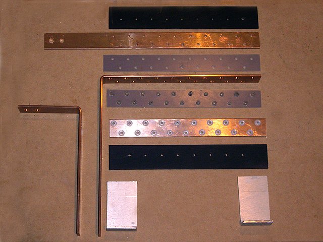
Figure 52. New Bus Hardware
The trick to getting everything accurately aligned is to mark out and drill the Drain Bus (second from the top) first. This then becomes your drill guide for almost all of the remaining 120+ holes. I recommend that you drill everything flat before starting to bend stuff, but maybe you know a better technique? Your can reduce your drilling effort by clamping some elements together - but try to avoid mixing soft materials with hard materials or you might have some rework to do. For all of the larger holes (there are a quite a few at 4 and 6 mm diameter) pilot drill at 3 mm or less and then over-drill to maintain accuracy.
I can see you asking, what are those two black things in Figure 51? They are aluminium thermal radiators with thermal inertia (in other words - heat sinks).
But my own calculations show that I don’t need heat sinks!
Just because they are not required doesn’t mean that it isn’t prudent to have some heat sinking. Cars don’t need seat belts but when something goes wrong they can be more than an optional accessory. The calculations are based on an ambient temperature of 25°C with no consideration of component thermal tolerances. A simple, low cost heat sink will significantly increase thermal inertia for transient conditions, and significantly improve heat radiation, convection and conduction (the shiny surface on the back of a power MOSFET is about as far from an ideal radiator as you can get). Let’s face it - other stuff in the case is getting hot (the charge board in particular) so ambient isn’t outside air temperature in the shade any more. Further, the MOSFETs are relatively expensive so why put them at risk? Finally, industry guidelines for conservative design recommend reducing maximum ratings (such as Tjmax) by 30% or more. So I am using a few simple heat sinks - albeit just strips of 3.15 mm thick aluminium painted with matt black engine enamel spray paint. As an aside these heat sinks will also improve the mechanical integrity of my design. Wait until you see it assembled!
Referring to Figure 52 from top to bottom we have:
top side heat sink (3.15 mm thick aluminium painted matt black).
drain bus (3 x 25 mm copper)
insulator (0.7 mm thick single sided FRP printed circuit board)
source bus (3 x 25 mm copper)
insulator (0.7 mm thick single sided FRP printed circuit board complete with plastic insulating inserts cut from 1.5 ml syringe bodies)
gate bus (3 x 25 mm copper complete with nylon insulating washers)
bottom side heat sink (3.15 mm thick aluminium painted matt black).
mounting brackets (less insulators and yet to be drilled)
Far Left, Ground bus connected to C+ and the positive weld electrode.
I am reluctant to drill the mounting bracket holes until Santa finally delivers my capacitors. This is a bother because everything else is ready for assembly. Please note that all of the mechanical drawings associated with the bus structure will be published at the completion of this project.
21 December and my new discharge MOSFET bus structure has been assembled as shown in Figure 53. Note that the weight distribution is about right even sitting on carpet. My original mounting brackets weren’t up to the task so I have replaced them with some recycled copper bus. The MOSFETs have yet to be inserted, the copper buses need to be cleaned, and I have a heap of machine screws to cut to length but you can see how it all fits together. In making this I have reused some of my earlier bus structure so there are a few extra holes where there shouldn’t be. The reduction in area and length over my initial effort means that, with rearranging of the the other assemblies I can now fit a third capacitor in my recycled computer chassis and get the charge heat sink aligned with, and closer to, the cooling fan. This is all good news but without any real capacitors I still can’t make those critical stud welds. Tomorrow I hope to be repositioning the subassemblies, mounting the MOSFETs, optimizing air flow from the fan over the charge board heat sink, and recalculating the snubber components on the gate drive to ensure no transients.
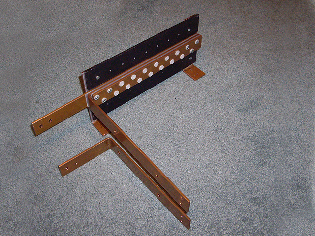
Figure 53. New Bus Structure less a few MOSFETs
With fast (tens of nanoseconds) switching speeds the distributed (as opposed to lumped) reactance of the gate drive and discharge paths may result in oscillation. While this has not been a problem for me yet, a simple method of suppression is an appropriately specified ferrite bead on the gate lead of every discharge MOSFET. This acts as a shorted turn at the oscillatory frequency damping resonance. The inductance of my current bus structure is minimal so I’ll hold this card up my sleeve until necessary.
Merry Christmas everyone! 25 December and Santa has come and gone here in New Zealand but I still don’t have my capacitors. I have started putting everything back in the recycled computer case (Figure 54) and with the new discharge MOSFET bus and a change in charge/discharge board heat sinks I have space to rent.

Figure 54. New Layout and Improved Design
(control, MCU and discharge drive boards not shown)
The charge and discharge boards are now mounted on one of my old main discharge heat sinks with almost twice the thermal mass of the earlier design. The recycled heat sink has been slightly cut down and horizontally mounted, with the charge board directly in front of the cooling fan. The main power supply capacitor has been changed to a taller but reduced diameter 47,000 uF, 63 V device. I dusted off my M3 tap and got rid of a whole heap of those badly positioned nuts (see Figure 23 above) making assembly a breeze, and incorporated some aluminium plate in the chassis to ease mounting and make everything a whole lot more rigid. I have also made two bus extensions for the third capacitor (I should have incorporated these in the initial bus design but failed to appreciate how much room I was making with the new layout). There is even room in the case for two further capacitors stacked in a pyramid on top of the existing three - whoop! (5 real Farads).
The main transformer position will be moved tomorrow to make it central with the rectifier, and I will be moving the chassis ground termination (a single point ground) to make it more accessible. The final tasks will be mounting the main discharge MOSFETS on the bus, ensuring transient free gate drive, and reducing a heap of lead lengths. Hopefully I will be back making sparks by tomorrow evening, albeit with just 0.9 Farads, but with significantly reduced discharge path impedance (resistance and reactance).
27 December and everything is reassembled and working. Figure 55 shows everything back in the chassis and Figure 56 shows the fully assembled main discharge MOSFET bus. There are no signs of oscillation and the weld pulse transients are nice and clean as shown in Figure 57. The resistance of the discharge bus structure has been reduced to about 0.002 Ohms. The charge heat-sink is running significantly cooler than before and there is no perceptible temperature increase in the main discharge MOSFET heat sinks.
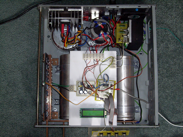
Figure 55. Reassembled and Working
Only two ‘faults’ occurred during reassembly. The first was a source gate short on the discharge bus identified with an Ohm meter check before any power was applied. At first I thought I was going to have to pull the bus to pieces, but a visual inspection identified that a gate lead hadn’t been adequately pre-formed and was in contact with the source bus. A quick pry with a scriber and the short was cleared.
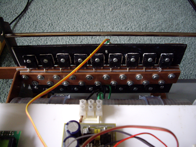
Figure 56. MOSFET Bus Fully Populated with 17 IRFP3602’s
The second ‘fault’ is a consequence of the extra capacitor and the relatively high leakage of the Boss capacitor above about 15 V. Hardware failure detection looks for a change in capacitor voltage during any charge or discharge cycle. With the increased capacitance the voltage change with constant current charge or discharge over 5 ms is about 30 mV. By the time this has been through a resistive 10:1 divider the resulting 3 mV is right at the resolution limits of the 10 bit ADC. The fix has been to extend the charge and discharge cycles to 10 ms. I still get an occasional error after repeated discharges from 15 V or more. I suspect that this is a simple consequence of the increased Boss capacitor leakage.
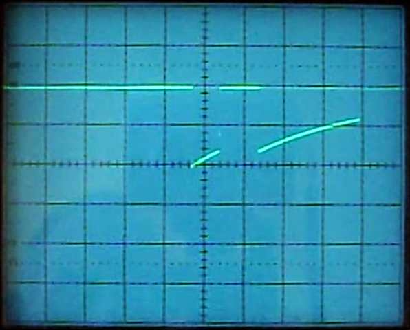
Figure 57. Discharge Measurement. Horz. 5 ms/div. Vert. 5 V/div Rload = 0.01 Ohms
P1: 3.5 ms, D: 5 ms, P2: 13 ms. CVSet = 12.0 V. Peak current = 1,000 A
(compare with Figure 42 above)
To finish the day I have made a few more welds. As you might expect none of these recent changes have added significantly to the available energy and as a consequence my welds are only slightly improved on my earlier attempts and not yet as secure as I’d like them to be.
Interlude
I am still waiting on my capacitors so it’s time to have some fun! Before the days of hockey-puck sized medium voltage semiconductors the world of power electronics ran on thermonic devices (valves, or if you live in America, tubes). Indeed many commercial radio transmitters still use valves in their finals. Figure 58 is a classic example of a (can you guess what it is - the colour should help) running at a rubber manufacturing plant. This is the biggest one of these that I have ever come across with a diameter of almost a meter (say 3’). The glasswork is truly elegant and I love the blue glow (to hell with the power efficiency) but I’m rather glad that the glass didn’t break while I had access. While there is no prize for a correct answer, I’m looking forward to your feedback on this (Contact Me).
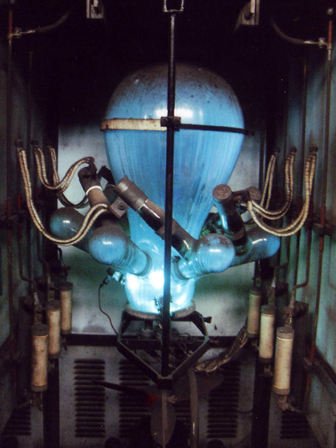
Figure 58. Looks Extra-terrestrial but was Conceived and Made by Mankind - So What is it?
More Trivia
As a fun exercise I thought I might calculate the theoretical capacitance of my Boss crapacitors (all credit to Mark for this terminology and as the first, and only, person to correctly identify Figure 58). Their physical construction is essentially two aluminium plates separated by paper and wound in an Archimedian spiral. The effective plate area of these crapacitors, taking into account the doubling effect of spiral wrapping, with 0.04 mm thick paper and aluminium, and the dimensions of the can is about 1.25 square metres. The maths is a little scary because of an inverse hyperbolic sine (ASINH in Microsoft Excel) but feel free to check this out on the Interweb. With optimum state of the art etching the surface area is increased by about 120 times. The dielectric is aluminium oxide (let’s be generous and say k = 9.4 ) with a thickness of between 0.0013 and 0.0015 um/V (again, let’s be generous and assign the lower value at 18 V). When I went to school the capacitance of parallel plate capacitors was:
C = k * Eo * A / t
where C is the capacitance in Farads,
k is the dielectric constant of aluminium oxide
Eo is the permittivity of free space, 8.854E-12 F/m
A is the effective plate area in m^2, and
t is the thickness of the dielectric in m.
When we plug the (conservatively estimated) numbers in we get a maximum of 0.53 Farads per Boss crapacitor. What is interesting is that this is remarkably close to their their actual measured value of 0.34 Farads (see above) before they started to self-destruct while being used well within their ratings.
I can only conclude from this that Boss crapacitors are actually crapacitors by design. If they had actually filled the aluminium case with capacitive elements and electrolyte with an allowance of say 10 mm for case insulation and 20 mm for electrolyte sealing then they would have been close to tolerance (within 5%). There is no way that these components could ever achieve a capacity of 2 Farads. I have placed an order with Mark for some real capacitors as my order from Sonic’s hasn’t arrived and I need to be making some progress here. I understand he has a few more available so if you are contemplating making a welder then you might consider sending him a polite email asking if he can supply.
On ESR, Carbon Double Layer (Ultra) Capacitors, and Hybrids.
I have two sets of capacitors on order now: some real electrolytic 1 Farad capacitors and two hybrid 2 Farad Capacitors, both made by Rockwell Fosgate. It has been explained to me that the hybrid capacitors won’t perform well in welding applications because they consist of half electrolytic and half carbon double layer (ultra) capacitors. I have already advised the supplier that I will be returning these if they don’t measure up to specification (18 V surge, 2 Farads and an equivalent ESR of 3 milliOhms). The issue that I am faced with is determining the actual ESR of the ultra-capacitors without opening the can. Ultra-capacitors have a typical maximum voltage of 2.7 V so assuming Rockwell Fosgate has been conservative in their design we can expect seven of these in series. If you go searching on the www under Ansoft you will find an equivalent lumped electrical model (Figure 59) of a ultra-capacitor that (on the basis of their reported experimental work) provides a reasonable approximation of actual electrical performance.
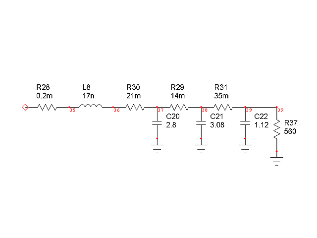
Figure 59. Lumped Model Ladder Network of a 7 Farad Double Layer Carbon Capacitor
(credit: Ansoft)
With seven of these in series a lower bound for the DC ESR will be R30 * 7 (ignoring R28 which is negligible) or about 0.15 Ohms. This is not good.
Figure 60 shows the theoretical discharge current curves for an 0.014 Ohm resistive discharge from a 1 Farad electrolytic in parallel with seven series-connected 7 Farad ultra-capacitors initially charged to 14 V. (Remember that this is a modelled response and is therefore not reality - although it should provide a reasonable estimate of actual response.) You can see immediately that the initial part of the response curve (black line) is almost entirely due the performance of the electrolytic capacitor (blue line) while beyond 100 ms it is determined almost entirely by the series ultra-capacitors (green line). The red line is the theoretical performance of a 2 Farad electrolytic with an ESR of 0.003 Ohms under the same conditions. This gives me a measurement technique to determine if I should return the Rockwell Fosgate capacitors against manufacturer’s specifications.
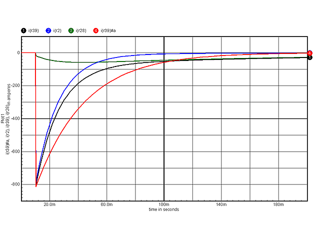
Figure 60. Discharge Current for Parallel Electrolytic and Ultra-Capacitor
Black: Current through 0.014 Ohm Discharge Resistor
Blue: Current contribution from electrolytic
Green: Current contribution from ultra-capacitor
Red: 2 Farad, 0.003 Ohm ESR electrolytic response
This exercise raises the issue of what actually constitutes a valid ESR measurement for ultra-capacitors because their distributed parameters mean they do not have a conventional capacitive exponential response. You can see from the green curve how the ladder network effectively smears the response out over time as charge is internally redistributed. While we can easily reduce the network shown in Figure 59 to an equivalent two port Pi or T section at a designated frequency (using simple reciprocal impedance’s and admittance’s using continuous fractions - a tedious exercise but doable) what frequency provides the best representation of welder response?
This confirms that using current technology, ‘small’ (say up to 10 Farad) series-connected ultra-capacitors is not going to work well in your welder - unless you put a lot of these in parallel. And with ‘small’ hybrids the ultra-capacitor element is not going to contribute significantly to useful weld pulse energy which is delivered in a few tens of microseconds.
Time for some Welding Practice
Although still starved of weld energy I have continued my weld experiments. I can now make consistently strong paper clip to washer welds (step electrode configuration) and have managed some 0.17 mm stainless steel sheet to stainless steel sheet welds (parallel electrode configuration with projections) where the stainless steel sheet rips before the weld nuggets fail. Just wait until I get some weld energy!
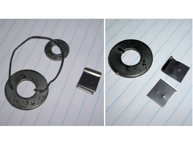
Figure 61. A few Good Welds (left) Proven by Ripping Apart (right)
My problem is that I don’t need to weld paper clips to washers!
6 January and I have been making progress on my other projects these past few days while awaiting arrival of some real capacitors. On review there is enough information above for you to duplicate my hardware and improve on my efforts (but please don’t make anything until my design is finalize and stable). If you can handle a soldering iron and apply appropriate safety precautions then you can build one of these without having to go through too much development. The following link will provide you with a copy of my AVR Studio assembler software under GNU GPL licensing. Please note that the processor board port assignments are hardware dependant as are the timing routines and you will need to provide the appropriate ATMEL standard definitions as an include file (included in AVR Studio).
As at today the current software version is E01.08 - the E stands for Experimental, 01 is the hardware, and 08 is the software minor variation. The code has worked with my current hardware for hundreds of welds now at discharges well in excess of 1,000 Amps, but that does not mean it will work with your hardware. I’ll be the first to admit that the code commentary is not great (actually it is lousy documentation) but I literally threw this together in just a few days. While certain sections of the code are optimized for precision timing the code is neither efficient, elegant or appropriately structured - but it works, and what do you expect for free? Figure 8 provides a reasonable top level overview of how everything is tied together. The hardware modules in my design are all CMOS/TTL compatible so you should be able to readily apply these to your favourite microcontroller with little difficulty.
For those folks that are truly fluent in C I must apologize for using assembler with this hardware platform. While I can write code in C, Pascal, Basic, Fortran, and a heap of other languages I was raised on binary (literally setting switches for the data and address buses, pushing the store button, and moving on to the next instruction). This was way back in the days when punched cards and perforated tape readers were new technology. If I want to write code quickly, ensure hardware control and timing accuracy then I usually revert to assembler. Sorry folks, but you can readily cut and paste this and adapt it to your your own platform without even having to type it all.
I intend to update and extend the code to include stuff like my cutting routines, power-on capacitor measurement, discharge energy display, and weld schedules in due course (none of these ideas are original - but my code is). You might want to check back on the download link from time-to- time to see if you have the latest code. (Please note that I have stripped out the watchdog and hardware test routines. These will be back in due course.)
Experimental Code: V. E01.09, 10 Jan 12.
(Posted on 10 January 2012 under GNU GPL provisions)
When my real capacitors arrive in the next few days I will be completing some hardware and weld tests and then publishing my entire design (board art work, bus hardware, BOMs, schematics, etc, all under free-ware licensing.
9 January and Mark’s 1 Farad Rockwell Fosgate capacitors have arrived (along with few 3 W LEDs which were totally unexpected - thank you Mark). The capacitors have a nice even weight distribution so I immediately suspect that there is no brick in these cans. They are full of capacitor and all three went straight in the case, a quick polarity check, refit the brackets, rewire the connectors, and finally reprogram the MCU for 15 ms charge and discharge pulses. All up this took an hour.
Welding time! The first stud weld to plated steel was rock solid. I had to twist it off with a spanner. Subsequent welds were also reasonably strong with CVSet at 10 V, P1: 2.5 ms, D:2.5, P2: 14 ms. This is really promising because I know how much better stainless steel welds have been and I haven’t even started playing with the weld schedules.
Time for some quick measurements. Figure 62 shows a test discharge with a brand new 0.01 Ohm test wire (the old one was looking a bit worse for wear). Compare this with Figures 42 and 57 above. The first thing you will see is virtually no droop during the discharge. The delivered power at the the end of P2 is within 15% of the start of P1. Excellent! There is also a slight transient overshoot of less than a volt during turn off. I suspect this is cable inductance combined with scope grounding.
We’re loosing about 2 V in this test which means a resistive loss of about 2 milliOhms including ESR, leads, buses and contact resistance. This is a significant improvement over my earlier 10 MOSFET design with resistive losses of 3.8 milliOhms.
I carried on making about 50 test welds - nothing is getting hot (except the welds) and no problems to report.
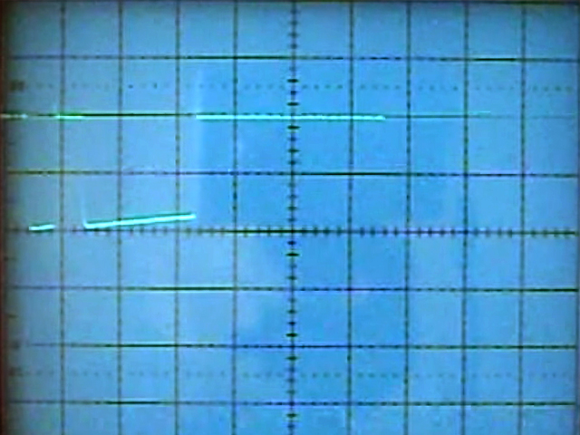
Figure 62. Discharge Measurement. Horz. 5 ms/div. Vert. 5 V/div Rload = 0.01 Ohms
P1: 2.5 ms, D: 2.5 ms, P2: 10 ms. CVSet = 12.0 V. Peak current = 1,000 A
(compare with Figures 42 and 57 above)
Now that I have some real capacitors its time to dissect one of those Quantum crapacitors and see what ‘clever’ stuff they have done on the inside. See Figure 63. Air isn’t a great dielectric, particularly when it isn’t even between plates. These crapacitors are 50% useless air!. The base is again refractory (looks like concrete but no ammonia smell). It is cylindrical with a height of about 40 mm and a diameter of about 70 mm. The capacitive element was about 120 mm long and just 35 mm in diameter. There was no noticeable free electrolyte in the can. The pitch seal was much harder than the Boss crapacitors. Just like the Boss variety there is no way that these Quantum paper weights could ever have a capacity of 2 Farads. I was wrong on one point - these aren’t made in the same factory as the Boss crapacitors - probably just in the same town. Boss would do well to study this image because they could reduce their pitch and electrolyte content by at least 50% and make even more money ripping people off with a product that is defective by design. Interestingly Boss have stopped corresponding with me. I wonder why? I will be writing some articles for auto-magazines in a short while to see if I can wind the pressure up on these fraudsters.
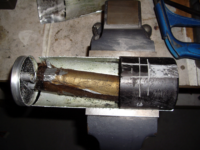
Figure 63. Sectioned Quantum Crapacitor
(Compare with Figure 39, a sectioned Boss crapacitor)
10 January and I have completed a minor software revision removing the watchdog and hardware failure detection routines because the former kept tripping during extended charge. The problem is that I need to keep the charge and discharge pulses relatively short (3 Farads charges about 50 mV at 10.2 Amps in 15 ms) to ensure accurate CVSet within 0.1 V and prevent overshoot. Because CVSet is measured through a resistive 10:1 divider we are now looking at a change of about 5 mV. While the processor’s ADC is 1024 bit from a 2.56 V reference its absolute accuracy is +/- 2 LSB (or +/- 7.5 mV). I am certain that during extended charge (like on power up) the main DC supply is sagging a bit under load, and particularly between half cycles. We are, after all, transferring energy from the power supply capacitor to the main discharge capacitors at near the rating of the mains transformer. This results in a reduction in Vds across the charge P Channel MOSFETs which are already operating in active mode. This reduces their current carrying capability which further reduces as they start to get warm.
What this all means is that the at the top end of an extended charge the charge current is likely to be dropping a bit which reduces our 5 mV in 15 ms - and the hardware alarm goes off followed by a watchdog reset. Not any more!
Time for some systematic development of weld schedules for my studs. I machined up a few dozen studs, set the welder for CVSet:12 V, P1: 2.5 ms, D: 2.5 ms, P2: 10 ms and made the first weld - looks good. Oops, I’d forgotten my notebook to record the results. When I got back just a few seconds later there was that horrible burnt semiconductor smell. If you persist with this project you will soon learn what I’m talking about sooner or later.
A quick Ohm meter check revelled a 5 Ohm short on the main MOSFET bus between drain and source. The charge board was right up to the task, continuing to hold the capacitor voltage at 12 V. This was my very first weld in this session so no components were hot. Nothing else for it but to take out the MOSFET bus and find what had gone wrong. 15 minutes later and I had identified and replaced the offending MOSFET. No significant damage other than my pride. The MOSFET case had cracked and melted a bit just above the source lead. Replacing MOSFETs every welding session isn’t really that much fun and will eventually become expensive. Time to think about what was different this time, and try and identify and solve the root cause.
Mark has previously suggested in personal correspondence that my fast gate drive may not be such a good idea because of the resulting high di/dt. There is an awful lot of literature on transient failure of MOSFETs and a number of possible failure modes.
Let’s start by thinking about what was different, and what was the same, today.
- First up I have some real capacitors. The voltage at turn is no different from what I had before, but at turn off the the current being switched is significantly greater than with my crapacitors. The discharge circuit resistive losses have also been significantly reduced (by a factor of 2) but the design change has done little to reduce the discharge path inductance.
- My previous test welds have been relatively resistive due to platings and the test material. The conduction path for this this weld was steel with bright clean contacts and a short discharge path.
- Unlike my earlier MOSFET failure which was directly (and physically) attributable to exceeding Tjmax there was nothing unusual about the mounting of this particular MOSFET.
- The gate drive is fine with no overshoot or transients and with an exceptionally low impedance (supported by actual measurements). There has been no change here for some time.
- With a 1,000 A discharge (resistive-load limited) you can see transients at the top of the rising edges (turn off) in Figure 62. With a significant reduction in load resistance during a weld these transient voltage spikes will be much greater than shown in the Figure. I have previously (and incorrectly) suggested that these are clamped by the MOSFET body diode. The drain is actually rising above ground and the body diode is therefore reverse biased at this time.
- I only destroyed one MOSFET. While this particular device may have been underrated I doubt it. More likely it protected the other MOSFETs by shorting from drain to source (a classic crowbar action).
- Looking way back at Fritz’s drive circuit in Figure 2 you will see that its turn off speed is relatively slow (about 0.25 ms). Perhaps he had a good reason for this?
My conclusion is that I have an inductive voltage transient issue cause by a fast high-current turn-off. Let’s throw some numbers into the mix and see if they will shed some light on the issue.
With a weld junction short the maximum device current, assuming shared conduction between MOSFETs is 18 V / 0.002 Ohms = 9,000 A (with equal MOSFET current sharing this is well within device Safe Operating Area, SOA). The gate drive is clean, and fast and so the rate of current rise is limited by the discharge path impedance to around 6.5E6 (that’s million) A/s.
We are switching our MOSFETs off in around 100 ns. The di/dt has just shot up to 90E9 A/s (and changed sign). If we assume about 2 uH in the discharge path, V = L di/dt = 2 uH * 90E9 A/s = 180 kV. The breakdown voltage between the drain and source, VBds, is 60 V minimum (but typically 130% of this value in avalanche). Okay, we have gone into avalanche. However this is not necessarily a problem provided that the avalanche energy is sufficiently limited. Unfortunately the devices that I have used and the discharge path inductance don’t pass this test.
This wasn’t a problem with the old capacitors because in any attempted real weld the current had reduced to just just a few hundreds of Amps after the first pulse. With real capacitors we still have significant currents flowing when the parallel MOSFET switch turns off.
So what can I do about all that energy stored in the discharge inductance and the resulting inductive EMF spike during turn off? Commutating diodes combined with snubbers and/or clamps across the drain source bus are the likely solution. Reduced MOSFET switching speed will also help.
At the currents we are interested in Ids is directly proportional to Vgs by Gm (note that this is a temperature dependant function). A simple low value non-inductive series resistor driving the parallel gate capacitance of about 0.14 uF (static measurement) will reduce the switching speed and di/dt.
As you might expect there will be an increase in the MOSFET power dissipation because of the slower switching speed. A quick linear estimate for a minimum pulse width of 100 us shows that the increased switching losses will be less than 5%.
Tomorrow I will be putting everything back together with the gate drive resistor and re-evaluate the snubber values. Then we shall see what else I can destroy.
This page is getting a bit long for ease of editing and uploading, and in any case you’re probably tied of reading the same old stuff. If you have read this far and want to read on then please click here to navigate to Continued Development.
|