|
I’ve been using laser printed artwork for making printer circuit boards for years. Prior to the advent of low cost laser printers I used either true photographic processes or Bishop decals and tape to lay the board out by hand on drafting cart (translucent) paper.
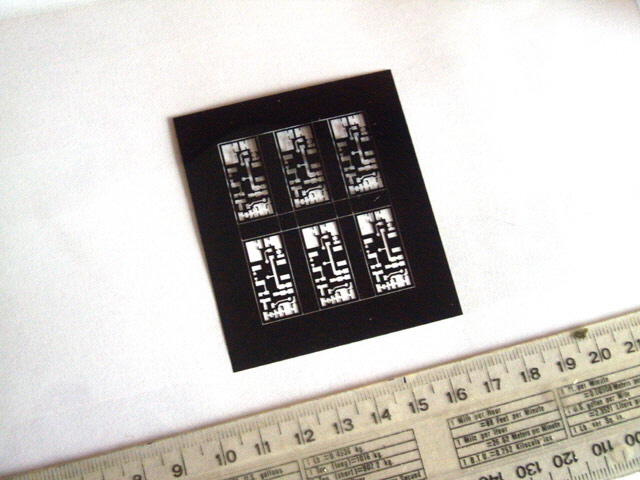
Figure 1. Typical Laser Printed Mylar Negative of Panel
Laser printed artwork on Mylar film is incredibly convenient, produced directly from your CAD package. But there are some potential issues that you need to be aware of.
Some Mylar film will thermally distort in a laser printer. The test for this problem is to overlay the Mylar on a paper print. They should correspond exactly. If this is a problem then either adjust your printer settings (the paper thickness may be too thick causing excessive fuser heating) or change your Mylar film.
The toner isn’t completely opaque. Change the printer settings to increase the contrast (and avoid toner saver settings). Check that the toner cartridge isn’t empty. Ensure the image is monochrome (not grey scale) and adjust the printer settings to suit. If this is still a problem then consider using two stacked negatives.
There are spots on the image. Check that the laser printer drum is clean and within the service life. This is likely to occur if you have tried to print on media that is not designed for laser printing. It is possible to re-polish a drum clean. Contact me if you want specific advice on how to do this.
There are stripes in the image. Check that the corona wire is clean (some printers provide a slider for cleaning this). Ensure that the toner is evenly distributed in the cartridge by shaking it gently from side to side.
The toner doesn’t adhere to the Mylar. This causes toner scratches and flakes during handling. and is caused by a low fuser temperature. Increase the paper thickness setting on the printer or select the Mylar media setting if it has one. If you still have a problem then find some thinner Mylar sheet.
Print at the highest native resolution of the printer. This should be at least 600 dpi, but 1,200 and 2,400 dpi should improve artwork resolution.
Orientate the image so the toner side will be facing towards the board (against the resist). This reduces blurring of the image beneath opaque edges.
Be sure to use clean, dust and scratch free Mylar film. Avoid handling the film in the image area both before and after printing.
Short of a vacuum table, apply a sheet of clean Perspex or glass on top of the artwork when aligning it to the board to remove any tendency for the Mylar to curl or lift off the board.
If you follow this guidance you should be producing good artwork, but chances are it will not be dimensionally correct. If you think about how a laser printer actually works then you should be amazed that it produces recognizable images at all, and not at all surprised that the image is unlikely to be the exact specified size.
Your laser printer should have an excellent aspect ratio but chances are that absolute dimensional accuracy is up to +/- 1% out. When you look at an image you will probably see when stuff isn’t square or circular when it should be, but for most images and text, absolute dimensional accuracy isn’t particularly important and is not visually discernible. The problem with using laser printed negatives for printed circuit boards is that dimensional accuracy is critical.
An 0.5% variation in printer accuracy will cause an 0.5 mm placement variation on a 100 mm wide board. Whoops, an 0.5 mm hole is fully offset in one or two dimensions with this much offset and probably cuts the associated pad wall. This is a disaster for through-hole plating unless the board is very small (say less than 20 mm x 20 mm) or the hole pads have a comparatively large diameter compared to the hole.
Even commercial boards will likely suffer from hole and pad alignment issues. Figure 2 shows a commercial board where the holes are displaced about 0.1 mm to the right of the centre of the corresponding pads. While this isn’t perfect it does not compromise the electrical integrity of the board.
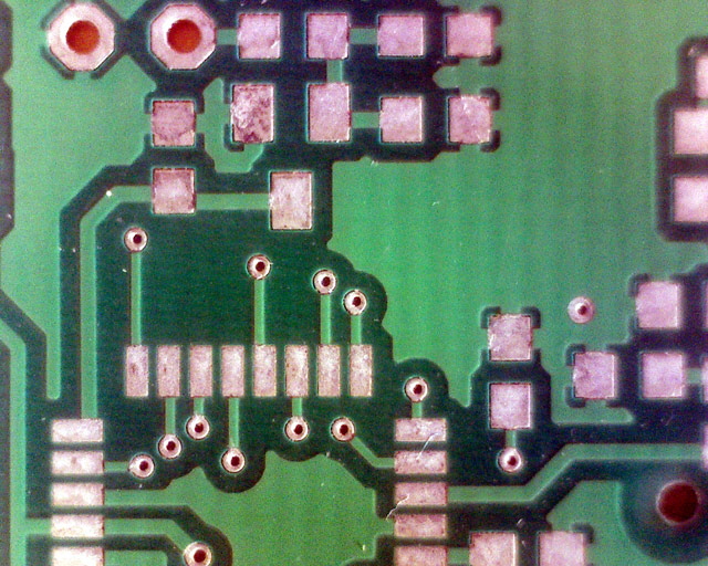
Figure 2. Commercial Board showing Hole and Pad Alignment within 0.2 mm
The following images show 0.5 mm diameter holes through 0.9 mm diameter circular, and SMD rectangular pads.
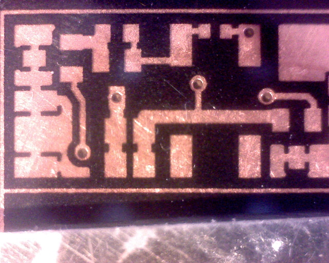
Figure 3. Top Left Board with Visually Aligned Holes and Pad
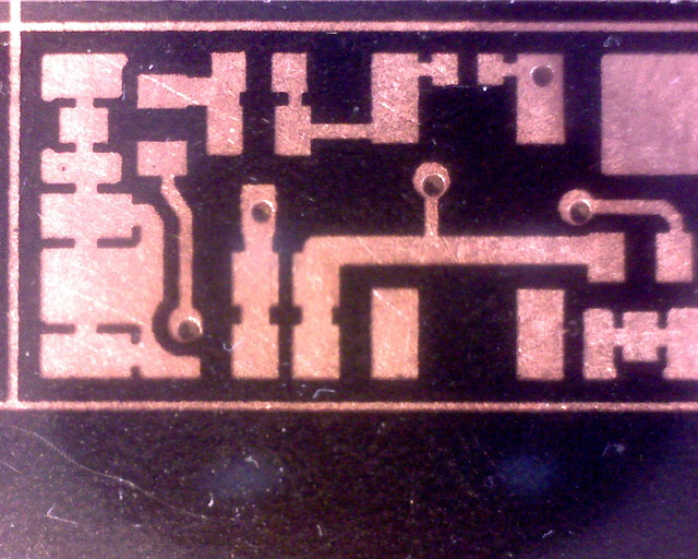
Figure 4. Bottom Right Board showing Unacceptable Pad and Hole Alignment
The laser printer mechanism uses a scanned laser beam to establish the width, and the drum and paper transport rollers to establish height of the image. While these may not be highly accurate they can be expected to be highly linear and repeatable.
Even with perfect artwork dimensions there will still be some (hopefully acceptable) error in the hole pad alignment because drilling, even with a CNC mill, introduces compounding errors. A hole is likely to have a location accuracy within +/- 0.2 mm with a CNC drill, but this will depend on a number of factors including the tool sharpness, feed and speed, machine rigidity, back-lash, and precision. And the hole itself is likely to be over-sized by up to 0.05 mm.
You cannot eliminate all compounding hole and pad alignment errors so, when designing your artwork, try and specify pad diameters at least 0.5 mm larger than the drill diameter.
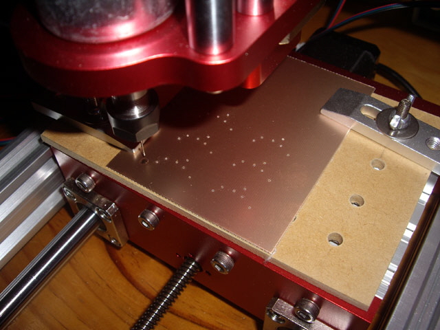
Figure 5. CNC Mill Drilling Operation
Manual drilling with an optical guide can reduce hole and pad alignment issues but this has its own set of problems with accuracy, is problematic for double sided through-hole plated boards where the process requires drilling prior to etching, and is time consuming.
The best remedy is to calibrate your printer and scale the artwork to compensate for dimensional inaccuracy. This process is relatively straight forward.
Draw a rectangle or square in your favourite CAD package at the largest board or panel size that you intend to make. This is likely to be a half Eurocard board.
Print the rectangle using your printer.
Measure the width, length and diagonals with callipers and calculate the scale adjustment which should be within +/- 0.5%. On my printer the scale adjustment is exactly 100.47% in height and 100.25% in width. Now apply this scale factor to all of your artwork in your CAD package. You’ll only need to calibrate the printer once, and perhaps after a change of drum unit.
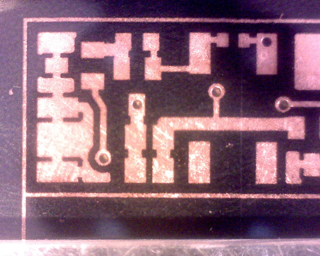
Figure 6. Top Left Board with Visually Aligned Holes and Pads
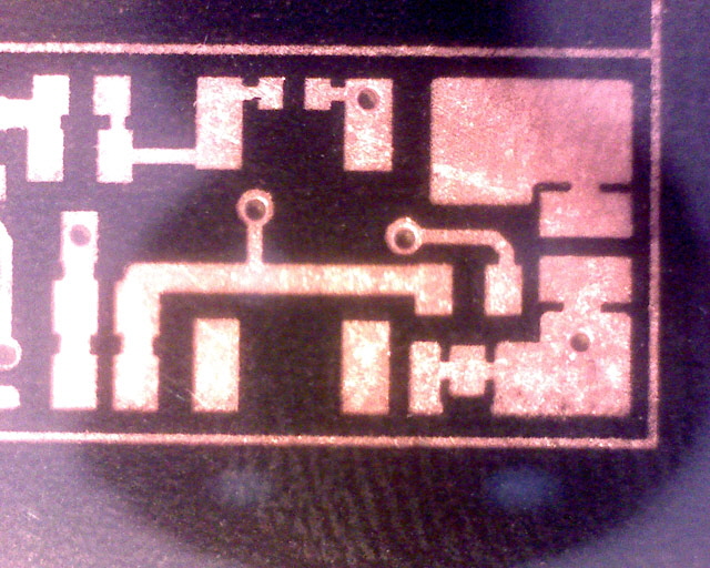
Figure 7. Bottom Right Board with Pad and Holes Aligned After Printer Calibration
Figures 6 and 7 show a significant improvement in the alignment of holes and pads after laser printer calibration (cf. Figure 4). While the alignment is not perfectly the board electrical integrity should not be compromised, and the holes are sufficiently central to ensure that the through-hole plating will be protected by the resist by tenting during etching.
|