|
I need a 36 Volt 5 Amp power supply for completing some tests on my 3D Hobby Mill.
I have made hundreds of power supplies over time, most of them linear, but I can’t even purchase the components for the cost of a Chinese sourced universal off-line 36 Volt 5 Amp Switch Mode Power Supply (SMPS) module at just over US$10 including postage!
I’ve ordered four, one for the experiment immediately on hand, and three for other projects (perhaps with some minor modifications to the module).
The modules arrived in just a few weeks. The packaging wasn’t great (anti-static bags in a bubble wrap envelope resulting in heat sinks being bent and but no critical damage was apparent. The core on one of the input inductive filters needed to be adhered to the frame to stop it rattling around.
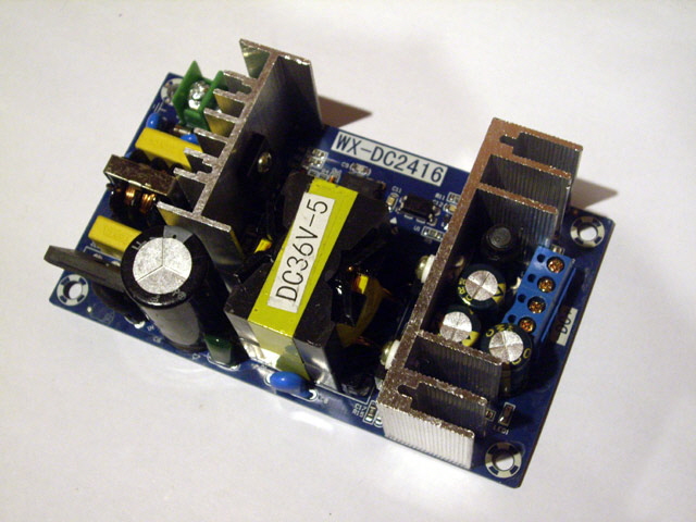
Figure 1. SMPS Module
The modules weigh about 200 g and have an envelope of approximately 115 mm long x 65 mm wide x 35 mm high.
Before I turn the module on let’s have a look at the design. The SMPS is based on the On Semi NCP1200P60 using a design similar to the Data Sheet, but with modifications as explained in Application Note AND8023. These include incorporating a TL431 precision reference in the feedback loop and an auxiliary primary transformer winding. The data sheet for this integrated circuit is not one of the most concise that I have ever read.
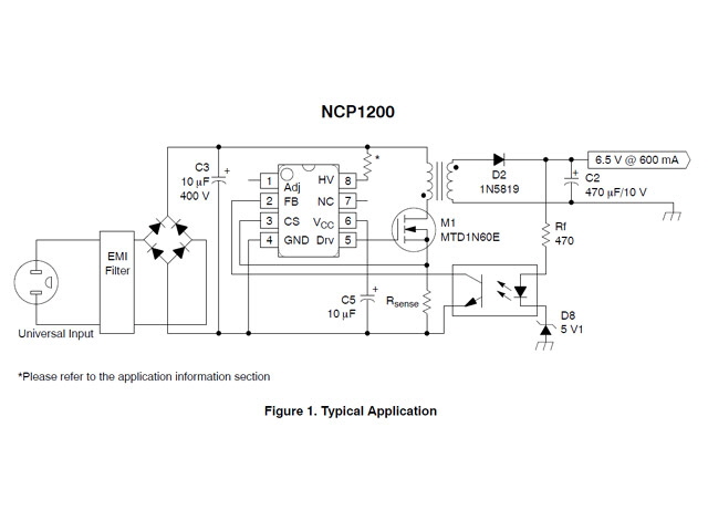
Figure 2. Schematic from On Semi Data Sheet
(Module is similar but not identical.)
The basic circuit consists of a mains filter and fuse, followed by a bridge rectifier and capacitive filter to produce about 325 V DC. This is then Pulse Width Modulated at about 60 kHz through a transformer by a 20N603C MOSFET rated at 650 V, 20 A, 200 W with a heat sunk fully isolated package.
The transformer has a singe output winding, bridge rectified by two heat sunk On Semi MBR20200 dual Schottky diodes rated at 200 V 20 A, and followed by a modest LC filter.
The primary winding has an axillary which is used to power the NCP1200P60. While this isn’t necessary it does reduce the quiescent current of the module as described in the Application Note.
The output circuit is fully isolated from the rectified mains by the transformer and opto-isolator feedback to the NCP1200 integrated circuit. The board layout provides good physical separation between the input and output with appropriate warnings of high voltage on the silk screen mask.
As previously noted, voltage regulation is achieved using a TL431 precision Zener and associated circuitry. Refering to the Figire below R2 is 20K and R7 is 1K5 which establishes an output voltage of about 36 V. We can readily change the module output voltage by simply changing one of these SMD resistors to acheive 2.5 V at the the Reference input to the TL431 at the desired output voltage. While this will alter the system dynamics I expect that the module will still function at rated current. We could improve the low voltage performance by adjusting the high frequency transformer secondary winding and the output LC filter but this is somewhat more complicated than simply changing out an SMD resistor!
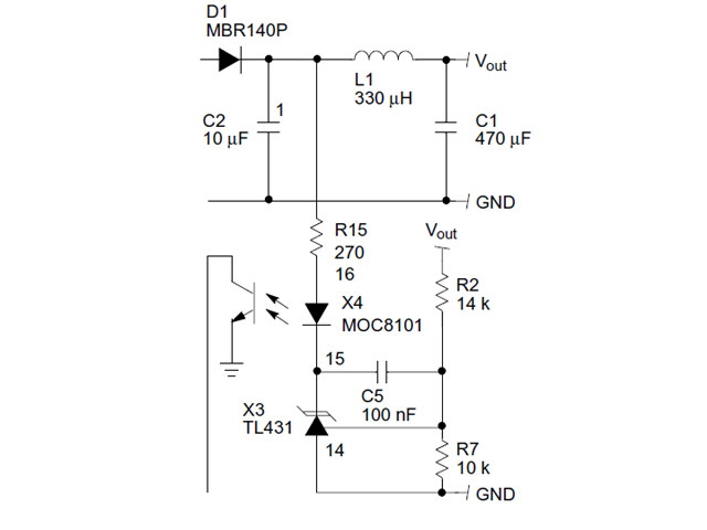
Figure 3. TL431 Zener from On Semi Application Note
(Module is similar with different component values.)
Current limiting is provided by sensing the primary MOSFET switch Source current. The NCP1200 also features cycle skipping to provide high efficiency under low load and thermal shut-down making for a very robust design.
I can’t visually determine if the board incorporates RC or RCD transient suppression around the main MOSFET switch and secondary rectifier without more detailed analysis. There are some sizeable low value SMD resistors, and some RC components near the switch and rectifier which I’m going to assume are for this purpose.
Interestingly, the board has a number of through holes directly under the heat sinks for convective air flow. This is good provided the holes are kept clear.
While SMPS like these can be very efficient, small and light weight, they may exhibit relatively high EMI and switching transients on the output. I will look at these once the module is appropriately shielded and in a case.
My initial thought was to make a simple 3D printed case, but I have found some old aluminium extrusions of an appropriate size. A couple of 3D printed end caps is all that is required to make a robust, safe and shielded power supply.
Here is the case, less lid, wired and ready for testing. The module is mounted on 10 mm long 6 mm diameter aluminium stand-offs which also provide an earth for the input AC filter. Rather than mess about making a cable clamp I have used a cable clamping grommet. There is lots of room in the case which measures 140 mm long x 90 mm wide x 58 mm high. The assembled unit weighs 700 g which is largely down to to the aluminium extrusion. I could readily make a smaller and lighter case but there is no need for the intended application. The additional weight will help keep the unit on the test bench.
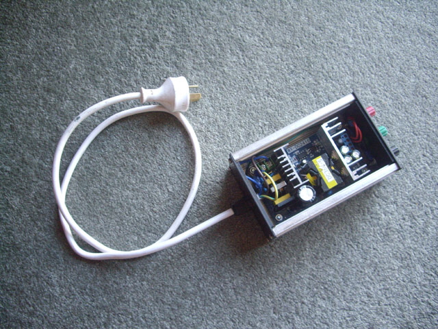
Figure 4. Supply in Case (less lid)
Testing
The first tests are case earth continuity, and AC and output isolation. We’re good.
The output is fully isolated so I have added a true earth terminal to the output connectors so we can have true +ve or –ve 36 V. For the following tests I have earthed the –ve terminal.
The open circuit output is 35.65 V. We can see the low load cycle skipping. There is a transient spike of about +/- 500 mV and less than 100 mV of ripple between cycle groups. The pulse frequency is quite low at about 48 kHz (60 kHz expected) and outside of the tolerance range for the IC (52 to 70 kHz). This suggests that the design uses out of specification or clone IC’s, but this does not appear to be detrimental to performance.
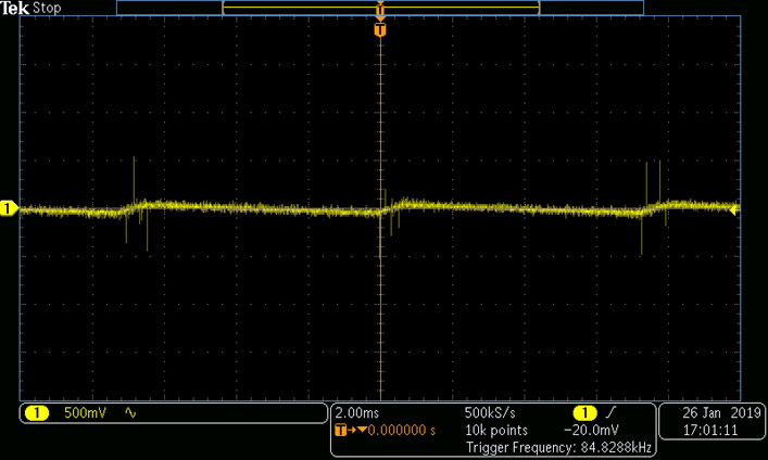
Figure 5. No Load Output. AC Coupled.
Time for some load. I’ve used a 1 kW heater element for this test because we’re going to be dissipating over 100 Watts. At a current of 4.2 A the output voltage is stable at 35.60 V.
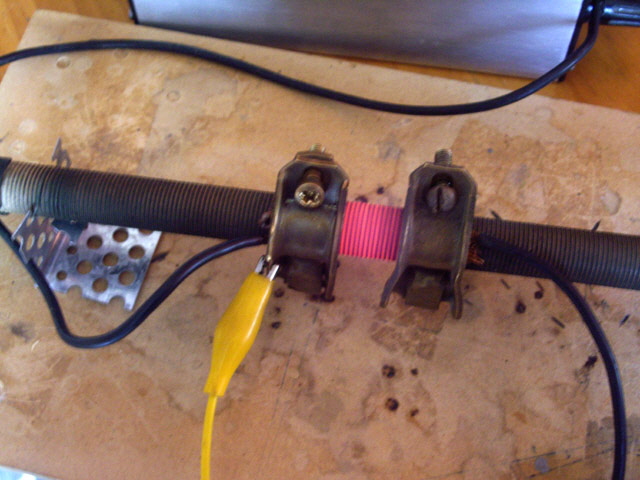
Figure 8. 150 W into 8.5 Ohms
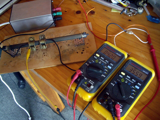
Figure 9. Load Test
(Note SMPS has lid fitted, top left.)
The transient spike amplitude has increased to say +/- 1 Volt, while the ripple has actually decreased. In the following figure the larger spike is the the off transition and there is quite a bit of ringing on the transitions. This suggests that, subject to other design constraints, the output current could readily be extended to 10 A and the snubber network has not been optimized. But we don’t need to go here just now as the circuit is performing quite adequately for its intended duty.
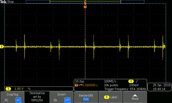
Figure 10. Load Test 4.2 A
The SMPS module is remaining nice and cool, even with the lid fitted and without ventilation holes after an extended period of load.
While I haven’t measured the effect of a transient loads I’ve appkied quite a few and the module is performing very well based on multimeter measurements.
Sure, I’ve had to add a case, mains cable, cable clamp, three terminals, a few nuts and bolts, but these bits were essentially all from scrap and 3D printed end caps were easy. A 36 V 5 A power supply in a case from a local distributor would have cost over $250 plus postage and packaging. Whoot!
Now on with my experiments…
|